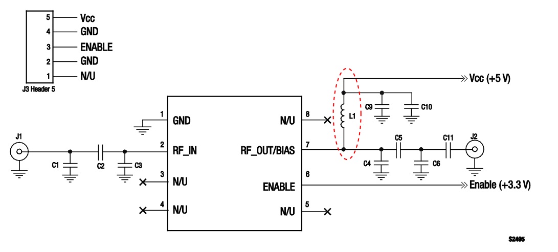
Why does the Vcc connect to RF path ?

Hi,
As attachment
Vcc connects to Pin7
L1 is RF choke to avoid making RF signal leak to Vcc path.
And C5 is DC-block to avoid making DC leak to RF path.
I have read the data sheet,
it describes this is related to bias.
Nevertheless, I don't know what is the detailed meaning.
Can anyone tell me what documents or books should I study to understand its detailed meaning ?
Thanks a lot~!
Simply output stage is open drain or open collector or like following.
http://www.avagotech.com/cs/Satellit...&ssbinary=true
bias is part of PA design. i would suggest you to study a book by steve cripps on RF amplifier design for more detail.
The pin, although labeled "Bias" (which has special meaning in linear amplifier design) actually provides the only path for DC voltage into the device.
For years I've seen this arrangement of applying voltage and I'm not sure if there's a performance advantage to doing it though the RF output pin.
Clearly, it has the potential for reducing pin count (and there are plenty of three-terminal amplifiers out there), but for the device in question above, there are unused pins.
- When to connect RF Bypass capacitor, and a Resistor in place of RF choke?
- How to achieve wireless connection between a resonator sensor and VNA?
- How do I connect / couple an oscillator to a bridge circuit
- can i connect 2 rf amplifiers to get higher amplification?
- Keysight ADS ground connection in schematic not reflected in layout
- Do you know the basic specification requirements for optical fiber connection?
