HFSS - PCB Antenna Design
I am designing a 2.4GHz PCB antenna (F-type). Snap attached. This design is already verified at 2.4GHz, since i have seen it in one paper.
I want to design similar kind of antenna for 2.4GHz and 5Ghz band, but before starting that I want to simulate existing designed and proven antenna and verify that my HFSS set up is correct.
I have few queries:-
1. What type of excitation I should give at feed? How should I give it? Should it be vertical from substrate bottom to feed entry point? Or there is some other technique to do that?
2. How should I connect patch to ground ? Shall I put gnd plane on top as well as bottom ? How to connect top and bottom plane to each other?
3. What should be other basic settings like Solution type?
4. Shall I take patch/gnd plane as sheet and then assign it as perfect E, or I make patch as a box of small height and assign it as PEC material?
Could any body help me in this?
Thanks,
Chaitanya
I don't know anything about PIFA antennas, but to try to answer your questions:
1) I usually use lumped ports.
2) Just bottom, I would think.
3) Max ~20 passes, deltaS = 0.01.
4) Depends on how accurate you want. I typically go with volumetric structures and assign it a material of copper.
Good Luck
Hello PlanarMetamaterials,
Thanks for your reply.
If I keep gnd plane just on bottom, how would I connect the patch gnd to bottom gnd.?
For assigning lumped port as feed, should I take it from substrate to feed entry point on top?
Thanks,
Chaitanya
I am using CIS STUDIO SUITE software for Antenna simulation.
Never add ground plane on top and bottom of the antenna. Antenna area should be free from Ground, Text, Metal etc...
I may have misunderstood your setup, can you post some images taken from different angles. What are you referring to when you say "patch"?

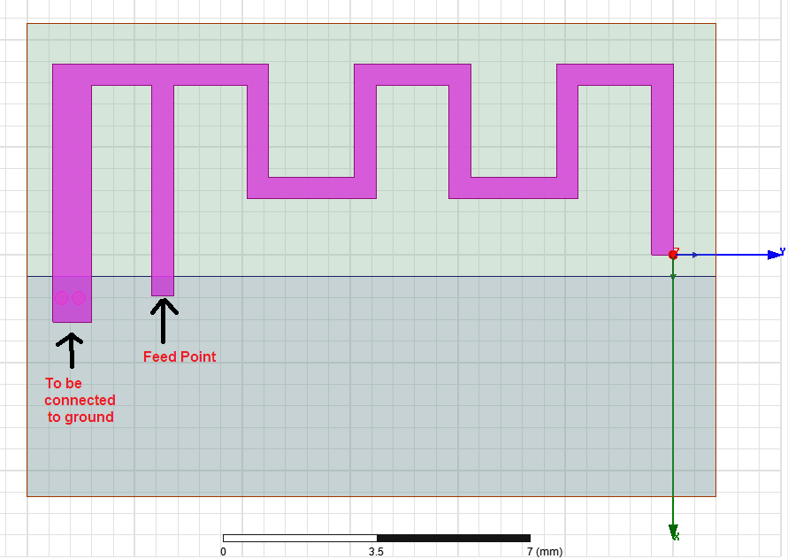
Attaching the snap., where highlighted area is what i am considring as patch