Realizing a J-inverter around 350 MHz
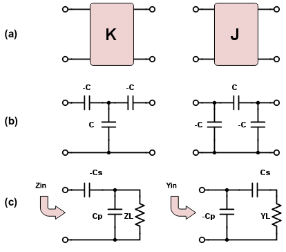
In previous applications in my work, we've needed inverters in low frequencies (1-10MHz) that are easily realizable using lumped elements. We use a half pi network which I show below for both K inverters and J inverters.

For the low frequencies this is easy because we can use 0201 surface mount capacitors to make our inverters; typically these are in the range of 100-10,000 pF.
For very high frequencies in the GHz, I understand it makes much more sense to use a quarter wave transformer for an inverter.
But I'm trying now to design an inverter around 350 MHz and the capacitor values to realize it are on the order of 0.2-6 pF! The error I introduce simply soldering these components on the board is on this order of magnitude; I find myself removing and adding on different capacitors of the same value until I get lucky with the tolerance. Clearly achieving my actual characteristic impedance/admittance is very difficult when it depends so much on hundreds of femto Farads. But this frequency still is too small for me to make a quarter wave transformer that can fit on our small device (~15 mm long).
Can anyone suggest a different way to realize inverters that I can design to a higher tolerance without leaving an enormous footprint on my device?
I have difficulties to understand the circuit schematic with your post as it contains non-implementable negative capacitances and inductances. May be you can show a physically plausible example of the filter circuits you are trying to implement?
I believe it's possible to design RF circuits with capacitor values accurate down to 0.1 pF. But it's necessary to include the circuit parasitics in the design calculation.
Ah, I suppose that is confusing. So all of these inverters are used to connect a load to a resonator, the negative capacitances are absorbed by the C in LC resonator, which is always large enough to accommodate. So a -1 pF would be absorbed by a resonant 5.0 pF resulting in a 4.0 pF parallel capacitor for the shunt resonator case. I'm having issues though placing a 4.0 pF capacitance instead of 4.1 pF, for example, and this detunes my system hurting performance.
Any help in designing high precision RF circuits would be hugely appreciated.
Perhaps, solution utilizing inductive inverter may be useful?
My concern is that the values will still be rather small, and that the lumped inductors will have a very low Q at these frequencies. Regardless its still something I haven't tried and could give me some more insight. Thanks!
You can expect Q around 50 at 350 MHz for wire wound air core inductor chips. You didn't yet which parameters you want to achieve.
Sorry, I'll give a test case.
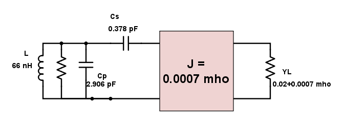
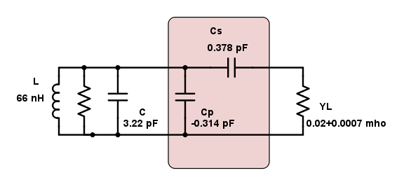
So I have a resonator with C = 3.22 pF (L = 66 nH), f0 = 345 MHz, Q0 = 50.
I wish to match this resonator to a load admittance Y = 0.02 + j*0.0007 mho with an inverter where J = 0.0007 mho. This results in a parallel LC with 66 nH, Cp = 2.906 pF, and Cs = 0.378 pF, where Cs and Cp are the series and parallel caps shown in part (c) of the figure I posted first. Note that the negative capacitance of Cp was absorbed into the original 3.22 pF resonant cap.

I added a parallel resistor in the circuit diagram to denote for the Q factor. For some background, the inductor is also magnetically coupled to a very high Q resonator (>1000), but I felt including that would distract from the system.
ADS simulations confirm that this results in exactly the value of J I need and gives me the performance I need. But even changing the capacitances by as little as 0.1 pF can detune my system. I feel as though I'm working at an awkward frequency regime where I'm too high to use lumped elements easily, but too low to use transmission lines.
I believe your matching circuit would be better understandable for common RF engineers if you gave a complete schematic with component values. Just take as granted that people aren't familiar with the J-inverter formalism...
To translate the matching problem to standard RF terms, you have nearly 50 ohm real impedance on the right side and a resonator with about 7 kohm parallel loss resistance on the left. In other words you are trying to match loads with about 1:140 ratio. It's the large impedance ratio that's makes matching by a LC network so sensitive to small parameter variations.
Ah, I'm sorry, I mucked up the circuit diagram. You're right, I'm far to used to dealing with filter abstractions and I'm a little removed from the circuits. That J inverter block is represented by the capacitors, this should show it more clearly. That last diagram is redundant.

Thank you for the insight, it did not occur to me at any point I am nearing the limit of feasible impedance matching. That would suggest a much more fundamental issue with my design.
