How to connect Instrument Amplifier to Differential ADC?
I used an Instrument AMplifier AD8226, which has IN+/IN-, but has only one output pin.
I want to connect it to ADS1292, which has two differential input and two 24-bit ADC.
How to connect it?
If I directly link AD8226 output to ADS1292 IN1P, and link IN1N to GND, is it OK if AD8226 output is positive pulse or negative pulse?
Is AD8226 can maximum support 16bit ADC or 24bit ADC?
Many thanks.
Best,
Tony Liu
Hi,
I Hope these may be of some help. ADC and op/in amp app notes and datasheets sometimes have example circuits, but none come to mind at present, I'm afraid.
Don't think you can have a negative going input if the ADC is tied to ground, that datasheet says the device can only go -0.3 below ..."VSS" or whatever term the datasheet used for 0V. What's the common mode range?
With no schematic it's even harder to understand the possible circuit.
Hi, d123 and others,
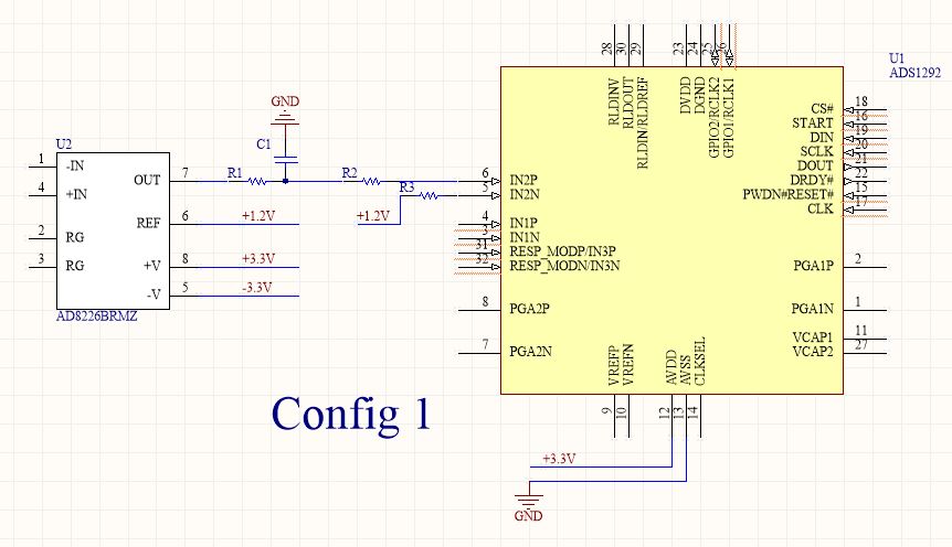
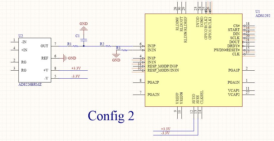
I figured out two solutions as the following.
In Config1, using CM voltage as 1.2V in both inputs of the ADS1292, which is for PGA, then ADS1292 using its internal VREF for ADC.
In config2, using single-ended input, but ADS1292 is configed to dual supply.
Which do you think can work?
Best,
Tony Liu
Hi, I think it's config 2, but I'm not 100% convinced of my reasoning...
The AD8226 datasheet says on page 10: "The output voltage of the AD8226 is developed with respect to the potential on the reference terminal. This is useful when the output signal needs to be offset to a precise midsupply level. For example, a voltage source can be tied to the REF pin to level-shift the output so that the AD8226 can drive a single-supply ADC."
And on page 11: "The output voltage of the AD8226 is developed with respect to the potential on the reference terminal. Care should be taken to tie REF to the appropriate local ground."
Which is why I think it should be config 2, adding that tying Ref and In2N to ground at the same point is probably advisable.
Hi, d123,
Many thanks.
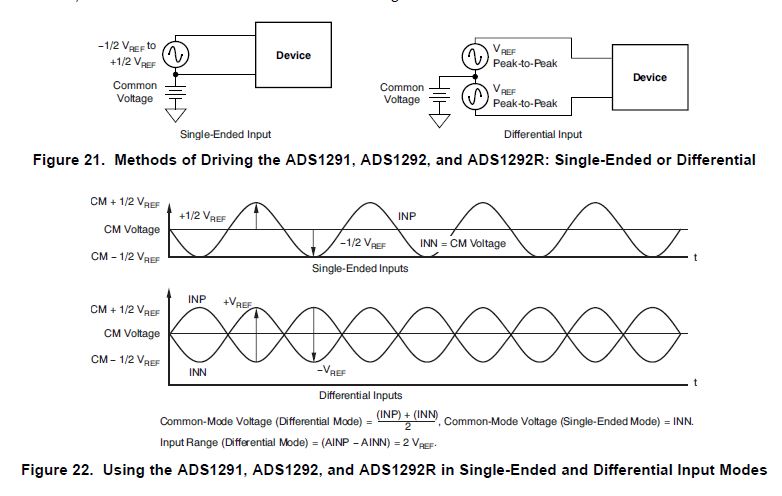
But I think COnfig1 is also OK, see ADS1292 datasheet with Fig21&22. Am I right?
Best,
Tony Liu
Hi Tony, I think you are right.
Hi, d123,
Thank you very much.
Best,
Like with most differential input ADC, ADS1292 datasheet suggests to use differential signal connection for best performance. But there are no quantitative data to estimate the actual benefit of differential mode. So we can just guess that there will be a certain linearity improvement. No idea if it matters for your application.
A differential input has many advantages. But you will see that the output is mostly single ended.
You must avoid ground loops as much as possible when connecting remote signals. However, you must use dual voltages for all amplifiers (so that the negative sides are also seen).
Hi, c_mitra,
ADS1292 has a PGA, so you mean that the PGA should be dual power supply with +3.3V/-3.3V? That is terrible, because I just want to give ADS1292 one +3.3V, no -3.3V. So that ADS1292 AVSS can link to GND for better noise, I guess so.
From ADS1292 datasheet, just above Fig.21, it says, "Note that the absolute range for INP and INN must be
between AVSS – 0.3 V and AVDD + 0.3 V. Refer to Table 10 for an explanation of the correlation between the
analog input and the digital codes. .... When the input is single-ended, the INN input is held
at the common-mode voltage, preferably at mid-supply. The INP input swings around the same common voltage
and the peak-to-peak amplitude is (common-mode + 1/2 VREF) and (common-mode – 1/2 VREF)."
So I guess Config1 aforesaid is OK when ADS1292 has only +3.3V power supply (no -3.3V ). Actually sometimes the waveform is negative sides.
Am I right?
I am looking forward to your reply.
Best,
In aforesaid COnfig1, INP and INN are surely between (AVSS-0.3V=-0.3V) and (AVDD+0.3V=3.6V).
Of course if the input does not have negative going signal, there is no problem.
Of course if the input is single ended (other one is ground), INN is held at common mode voltage, preferably at mid-supply- that suggests that the remote ground is lifted by about mid-voltage level
Hence the input must be limited to VREF*0.5 if there is a negative going component else VREF is ok.
Note that even in the single ended example, the other end is connected to a common mode voltage (not ground).
The ADS1292 datasheet is pretty clear about single supply operation. Whether you are using it with single ended or differential input signals, the absolute input voltage must keep the ADS1292 analog supply range, e.g. 0 - 3.3V (or 0 to 5V). An instrumentation amplifier connected in front of ADS1292 would be respectively biased to mid supply.
Hi, All,
The following picture is from ADS1292 datasheet. So when MuxP is 0V and MuxN is 1.6V and ADS1292 has only +3.3V power supply, the currnt is from GND to +3.3V, so act as negative current, right?

If the gain setting is more than 1, the input levels may be too high.
Instrument connect Amplifier 相关文章:
- When to connect RF Bypass capacitor, and a Resistor in place of RF choke?
- How to achieve wireless connection between a resonator sensor and VNA?
- How do I connect / couple an oscillator to a bridge circuit
- can i connect 2 rf amplifiers to get higher amplification?
- Keysight ADS ground connection in schematic not reflected in layout
- Do you know the basic specification requirements for optical fiber connection?