How to connect a matching network
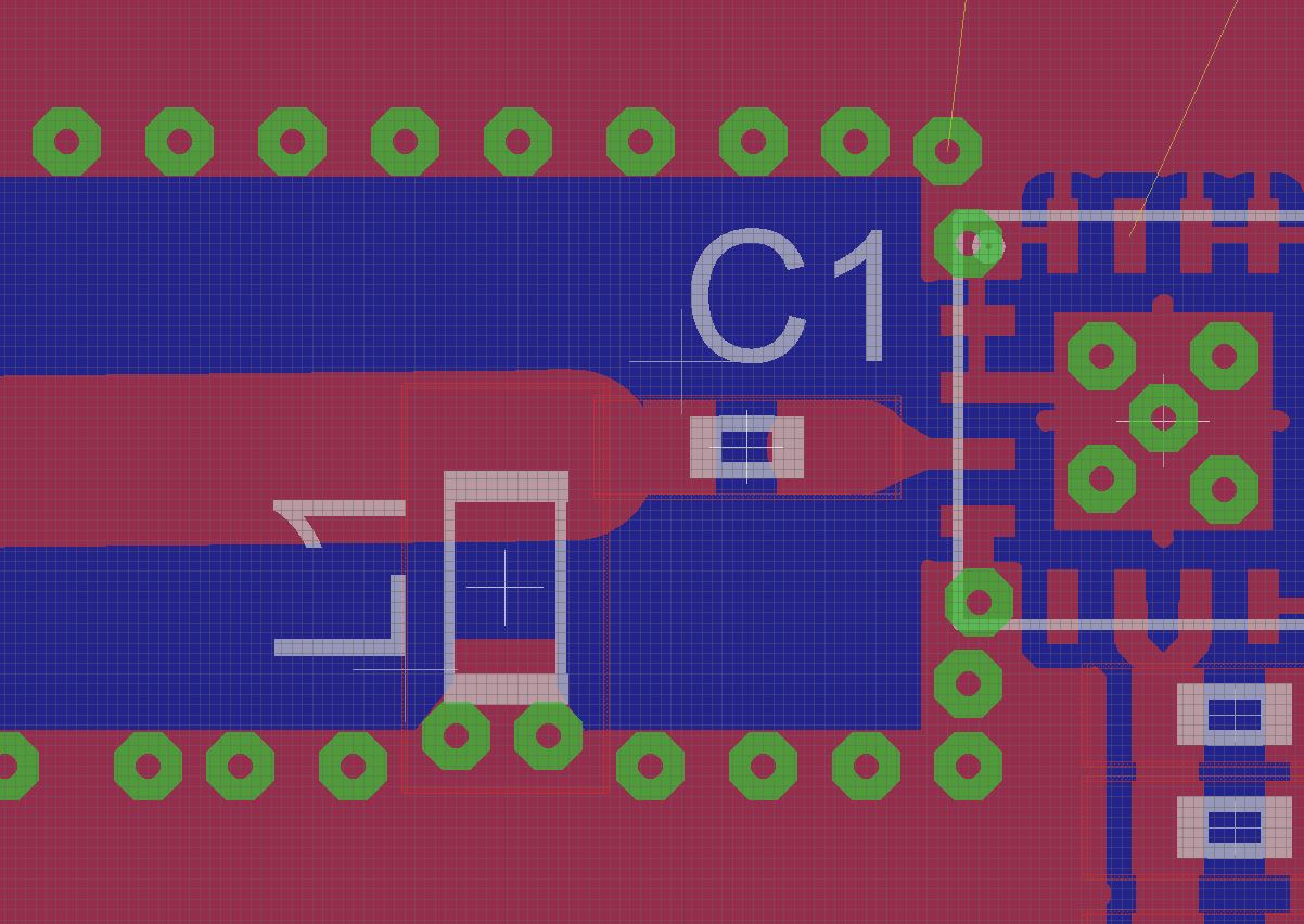
I am currently planning a transmission line for a received 2.4GHz signal. Unfortunately, I?m not very experienced with RF design. At college, I was attending a course of high frequency. But this doesn?t help me with my problem. I don?t know how I connect the transmission line to the matching network and the IC-Pin (mixer). The coplanar waveguide with lower ground plane (CPWG) is 1.60 mm (63 mil) wide. All smd pads are much smaller. Figures below show first ideas of the layout. How would you connect the components?
Thanks
iqFizz
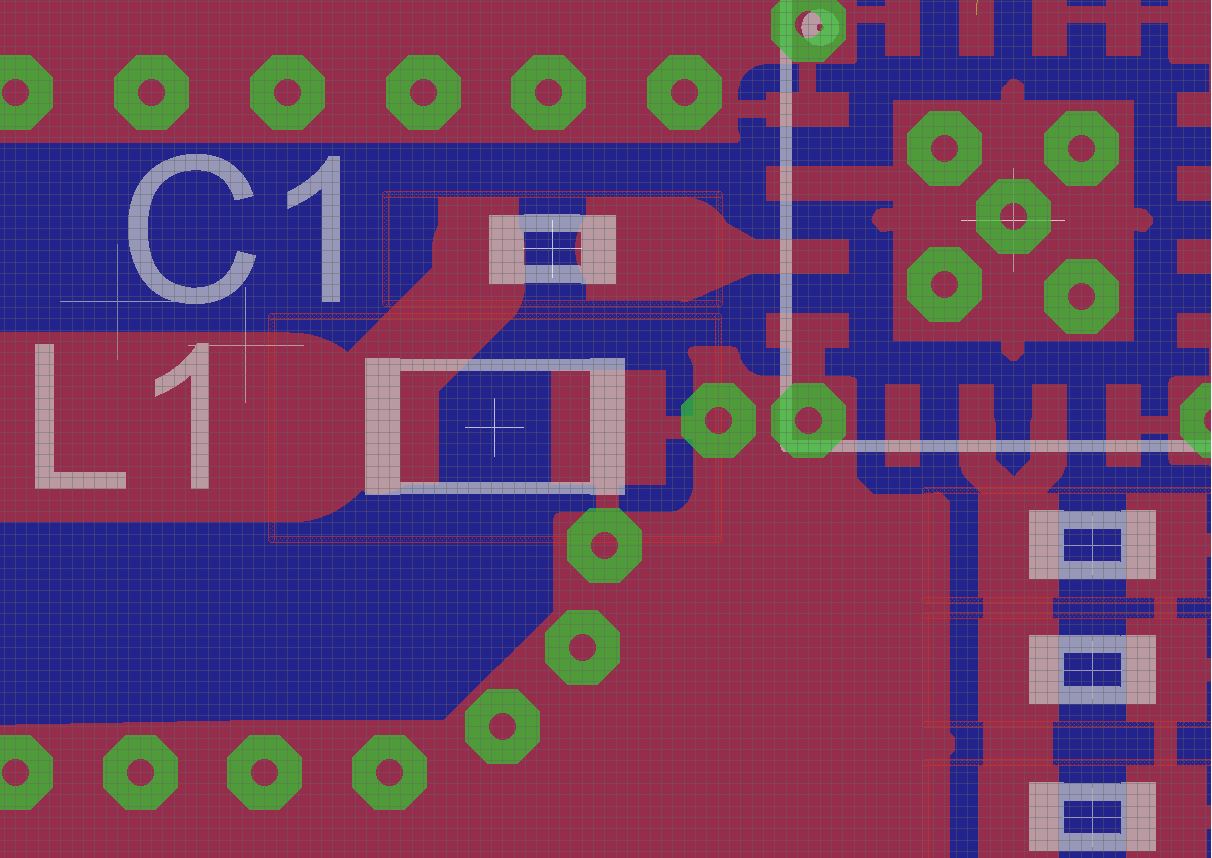
Don't use thermal spokes for RF PCB (L1 ground pad).
I don't see an actual CPWG structure, rather a micro-strip with distant ground via fence, impedance is mostly that of the pure micro-strip. You could however taper the center line and reduce the ground separation towards the end.
Or leave everything as is and put some series inductance for C1 into the calculation.
Hi,
For the 2.4GHz the wavelength is much larger than the discontinuity of the transmission line, so just keep the non-50 ohm part of the trace as short as possible. The layout on the second picture is much better than the first one, the only change I would make is to change the C1 footprint to be the same as L1, in this case you don't need to change the width that much to keep the 50Ohm.
R.
Thanks for your answer. I will try to simulate the transmission line with ADS.
What distance should be between signal and ground for a CPWG at the top layer? In this layout the distance is 1.8 mm. It’s 2.25 times of the substrate strength with 0.8 mm.
What is better CPWG or micro-strip on a 2 layer pcb. Unfortunately, the substrate is FR4 TG130.
connect matching network 相关文章:
- When to connect RF Bypass capacitor, and a Resistor in place of RF choke?
- How to achieve wireless connection between a resonator sensor and VNA?
- How do I connect / couple an oscillator to a bridge circuit
- can i connect 2 rf amplifiers to get higher amplification?
- Keysight ADS ground connection in schematic not reflected in layout
- Do you know the basic specification requirements for optical fiber connection?