How can I use pad for SMD components
In my design, I use some SMD components. when I consider pads for them, my simulation result (S21 and S11) is changed.
I apply the dimension of pad from datasheet. why do the results change?
So your operating frequency is too high right ? SMD pads should normally not change the response too much at moderate frequencies (1-2GHz ).
Either there are some calibration errors in your simulation setup due to very close ports or something goes wrong.
Can you post your layout and simulation setup ?
The frequency of filter is 2-4GHz
There isn't any error
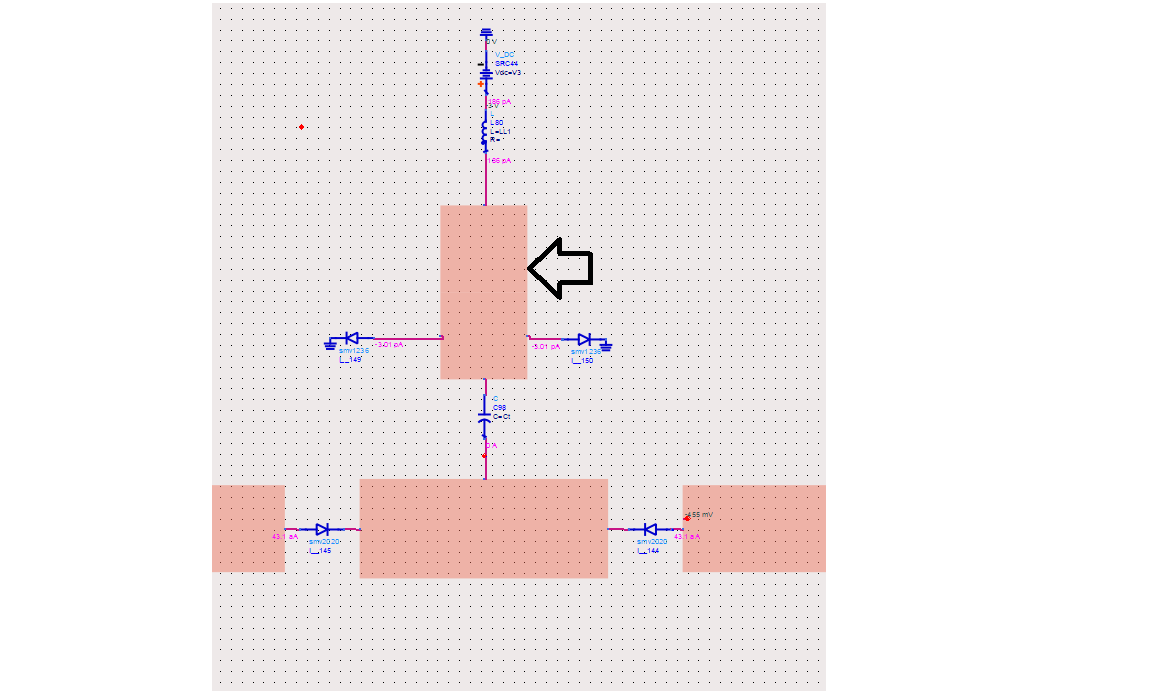
In below figure, when I use the shown cross pad, the results are changed
The pad creates additional capacitance to ground, and can also add length => series inductance.
Some measured S2P files for SMD already include the pad effect in the S2P data, for the pad size used in measurement. We do not want to include the pad effect twice, in the S2P data and again in EM. We want to include the pads only once, so must check documents for your components/libraries what they tell about the S2P data.
In your EM model, the pins/ports for EM are on the edge of the pad. The reference plane for SMD data can be in different places, often at the edge of the package. Package edge location is not pad edge. You need to adjust the EM pin/port location for this reference place. Depending on frequency and pad size, you also need to consider EM port style/size as I showed in this appnote: http://muehlhaus.com/support/ads-app...edge-area-pins
Welcome to real world RF circuit design. It's just normal operation. Any component pad becomes part of the distributed circuit and must be considered when modeling it.
It's not so easy to find out under which conditions S-parameters given in a component datasheet are valid, what are the reference planes and test adapter geometry.
All pads are ok and don't have any side effects but just this pad ruin the answer.
As you said, I should transfer ports from edge to inside of the microstrip line. Is it correct?
I don't know how large that pad is. Maybe you can check sensivity to small parasitic effects: try ideal circuit (no pad) and add cap to ground (some 100 fF) and series inductance (1nH or so).
Yes, but you also need to know more about your S-parameter references planes. If they include some pad effect already, you must remove the pad (fully or partially) from EM. It really depends on the S-parameter data measurement.
I don't understand what you said. How can I model the cross pad with L and C?
I should consider the pad for simulation because I want to manufacture and measure it
I did not mean that you model the cross pad with L and C.
My suggestion was to check how sensitive your circuit is to series L and shunt C at that circuit node. Then you know what type of parasitic effect is critical there, so that you can change the layout (pad).
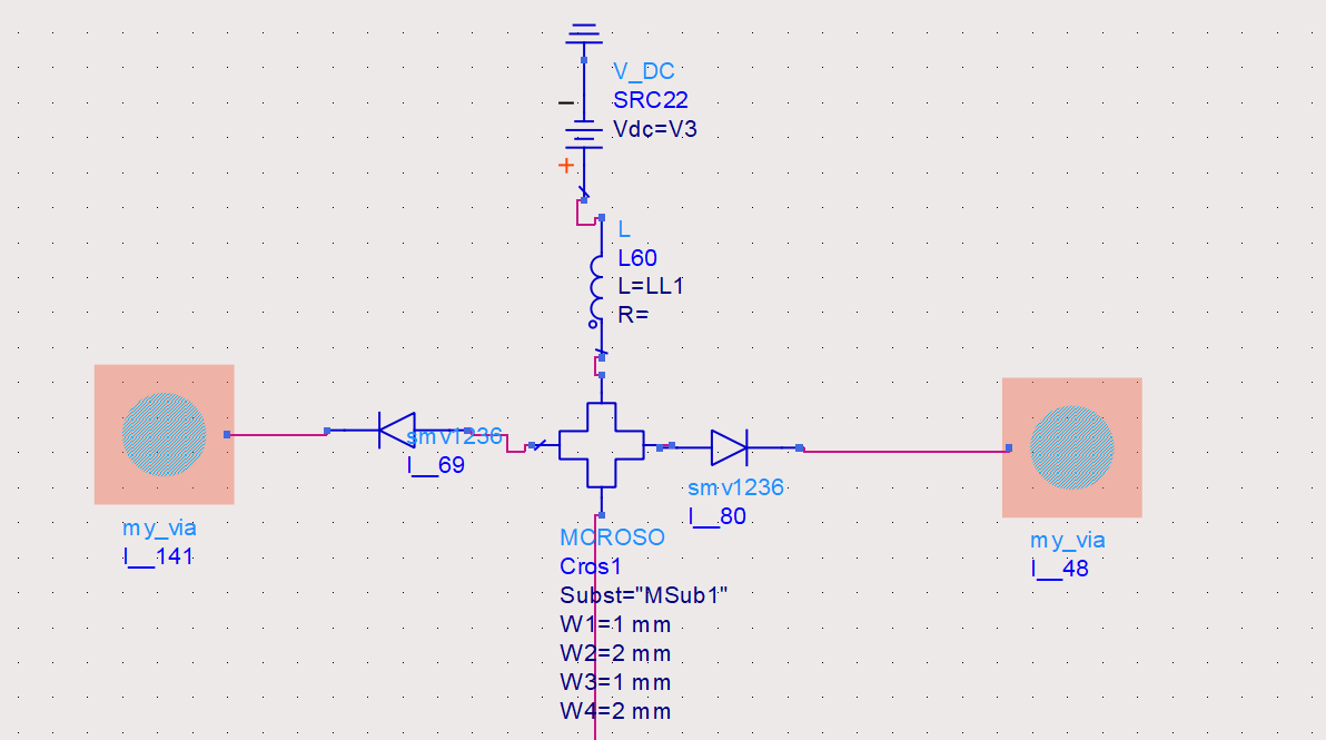
Instead of microstrip pads in Momentum, I use cross pad in the schematic page so the simulation results are better that the previous results
Sorry, this is not enough detailed information to support you efficiently.
But this is not a realistic point of view.What does it make sense if we use modeled schematic view of the distributed components ? How will you know the interactions between the pieces ?
In 18 years of EM support work, I have seen all sorts of user error in EM models. Sometimes it's easier to start from a simple schematic/lumped model, to see if an effect makes sense and might be real. That's why I suggested above to investigate sensitivity at this circuit node.
Of course, an accurate EM model would be great, but it seems that laperla doesn't know the S2P ref planes and measurement conditions, so that's a guess anyway.
I couldn't find any S2P models for applied components
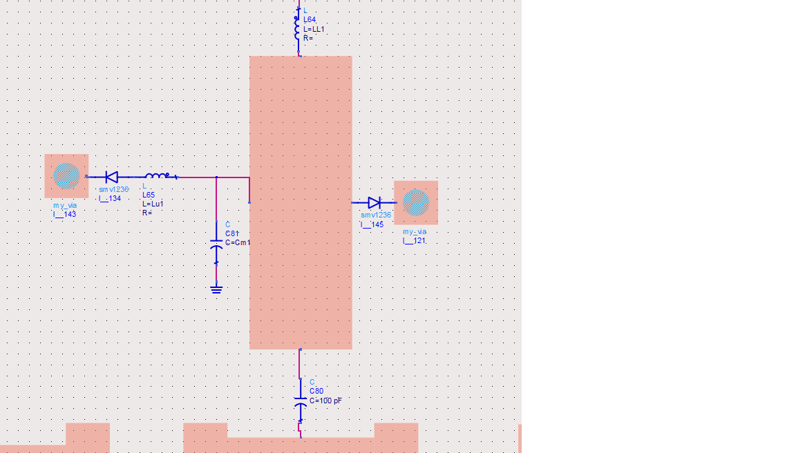
I used series L and shunt C in the node of a varactor. The results of simulation are better. It seems better but doesn't completely correct.
It's really difficult with your posts, we always need to guess guess guess what you are doing.
What means "better" and "correct", compared to what? Show curves, please.
What component uses S2P, and what uses other models? How do you model the diodes, ideal diode with no package model?
What values you use for series L and/or shunt C?
I compare the layout results with pad and without the pad.
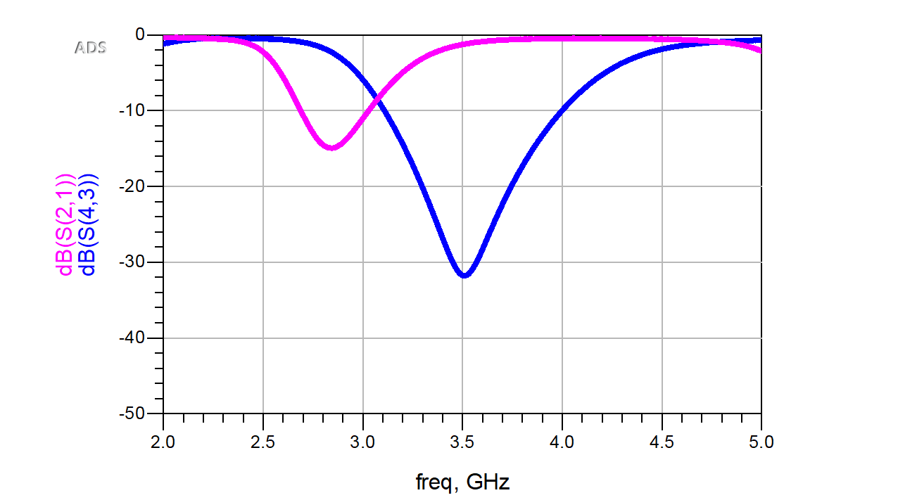
In this fig, the pink curve is with pads ( series L and shunt C) and the blue curve is without any pads
Diodes are varactors that I use the spice models for them. Other components is ideal I don't have any S2P models for thems
C =100pF and L=82nH
What is the size of the cross pad?
What substrate (epsilon, thickness)?
Does your diode model include the package effect (Ls) from the data sheet?


Then don't expect accurate results. You need to go back and find components with S parameter data in your frequency band, and use the same footprint as specified in the datasheet. Such documentation should be simple to find from good manufacturers.
The size of pad is 2*1 mm^2
The eosilon of substrate is 3.55 with thickness 31 mil
I used the SC-79 package with Ls=0.7nH
EM extracted parasitics for your pad:
Pad capacitance to ground is 0.18pF, which is small compared to the varicap path.
Series inductance from "bottom side" to "diode side" is 0.6nH (per path).
You can go back to your "ideal" schematic, insert these parasitics and see if that is close to the EM results with pads.
pad SMD components 相关文章:
- How to take ESD and pad capacitances into consideration during design
- Re: How can I use pad for SMD components
- SMD component fixture for antenna matching prototyping
- Checking 2 Port SMD Device for Passivity
- Why is there always a shunt inductor for SMD (Surface Mount Device) antenna?
- Would smd resistor on ridge waveguide (or rgw waveguide) act as series resistor?