Re: How can I use pad for SMD components
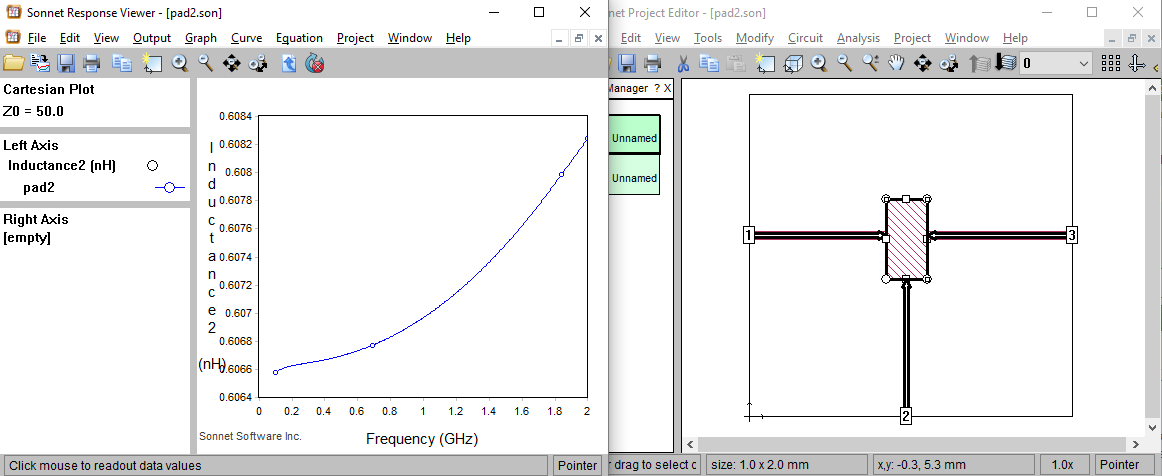
I used an EM solver to simulate the pad and then converted S/Y/Z parameters to equivalent component values. My reference planes are at the outer edges of the pad.
As said, this is only to understand what physical effect in layout causes the difference in results between "ideal" and "with pad". You can put in only the shunt C (represent pad shunt cap) and check, and you can put in only the series L (representing pad series inductance) and check results, and this helps to understand how sensitive your circuit node is to layout effects (series inductance from path length, shunt capacitance from pad area). Then you can make layout changes to minimize that effect, and re-tune the rest of the filter to work with pad included.
pad SMD components 相关文章:
- How to take ESD and pad capacitances into consideration during design
- SMD component fixture for antenna matching prototyping
- Checking 2 Port SMD Device for Passivity
- Why is there always a shunt inductor for SMD (Surface Mount Device) antenna?
- Would smd resistor on ridge waveguide (or rgw waveguide) act as series resistor?
- RF SMD attenuator makes RF path and Ground short.