Compare ADS Simulation and Application Note
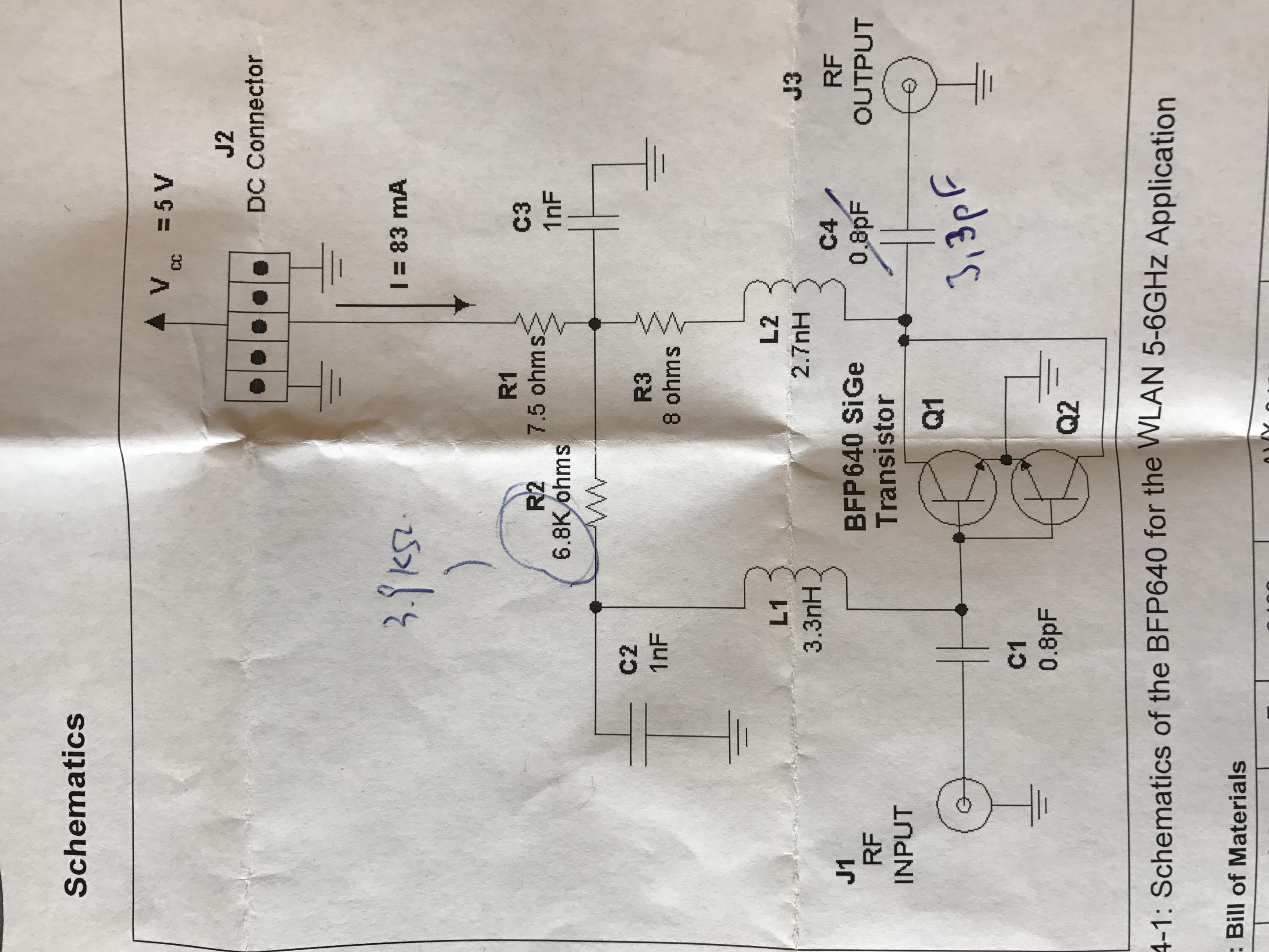
i am currently working on a paper about an LNA. In my work i wanted to compare the simulated results and the results given me by Infineon in their Application Note.
Now here is my Problem. I built exactly the device described in the AN in ADS and simulated it in the proper frequency range. But the AN says that there should be a Inturn Return Loss (S11) from about 19.8 dB in my desired frequency. But my simulated results give my a S11 value of 1.9 dB?
All the other parameter are in a acceptable range.

I hopy someone can help me figure out the problem here.
greetings
stephan
Did you confirm Vcc current ?
If it is 83mA, try to replace two inductors with realistic one.
http://www.murata.com/en-us/tool/lib...xxx_cmn_hd_xxx
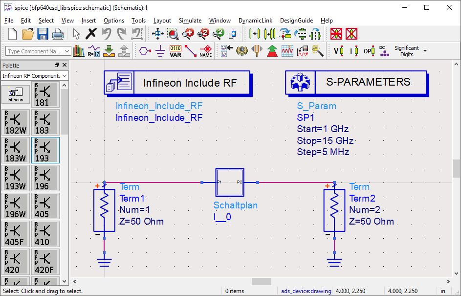
Do you surely terminate port=2 as 50ohm ?

as you can see i got 50 ohm on both ports. what do you mena with confirm the Vcc current? i only told ads that my source should got 5V as you can see in my first post. When i measured this board in the lab i put the source to 5V and only got 59mA, but the results were fine. the problem is that i cant compare both results because of the big difference
i meant my measured results from the hardware is good. but i want to compare the simulation model with the hardware model in my paper. and since i built exaclty what the AN said the difference shouldn't be this big
Operation point is different.
Reduce R2 value such that Icc is 83mA.
Or increase Vcc value such that Icc=83mA.
What do you mean ?
You post question here since your result is not good.
If your result is fine, close this thread.
Wrong.
Difference of operation point betwee Icc=59mA and Icc=83mA is very serious problem.
Do you mean Icc=59mA is actual measurement result ?
Show me Icc result of Simulation.
However I think your large discrepancy of S11 is due to ideal inductors.
Surely read https://www.edaboard.com/thread364764.html#2
Replace two inductors with more realistic.
You probably make a mistake when you use the model.There should be 2 models; One is small signal defined by s-parameters, other one is nonlinear.You probably did your simulations with the first one and therefore you find huge difference because using the first one does not make sense in a DC biased simulation set-up.This is my guess otherwise correct my statement.
You can not understand at all.
You use ideal inductor and capacitor in your simulation.
You can never get consistency between simulation and actual measurement as far as you use such ideal inductor and capacitor in your simulation, since your simulation is relative high frequency, 5GHz.
Show us Icc in your simulation.
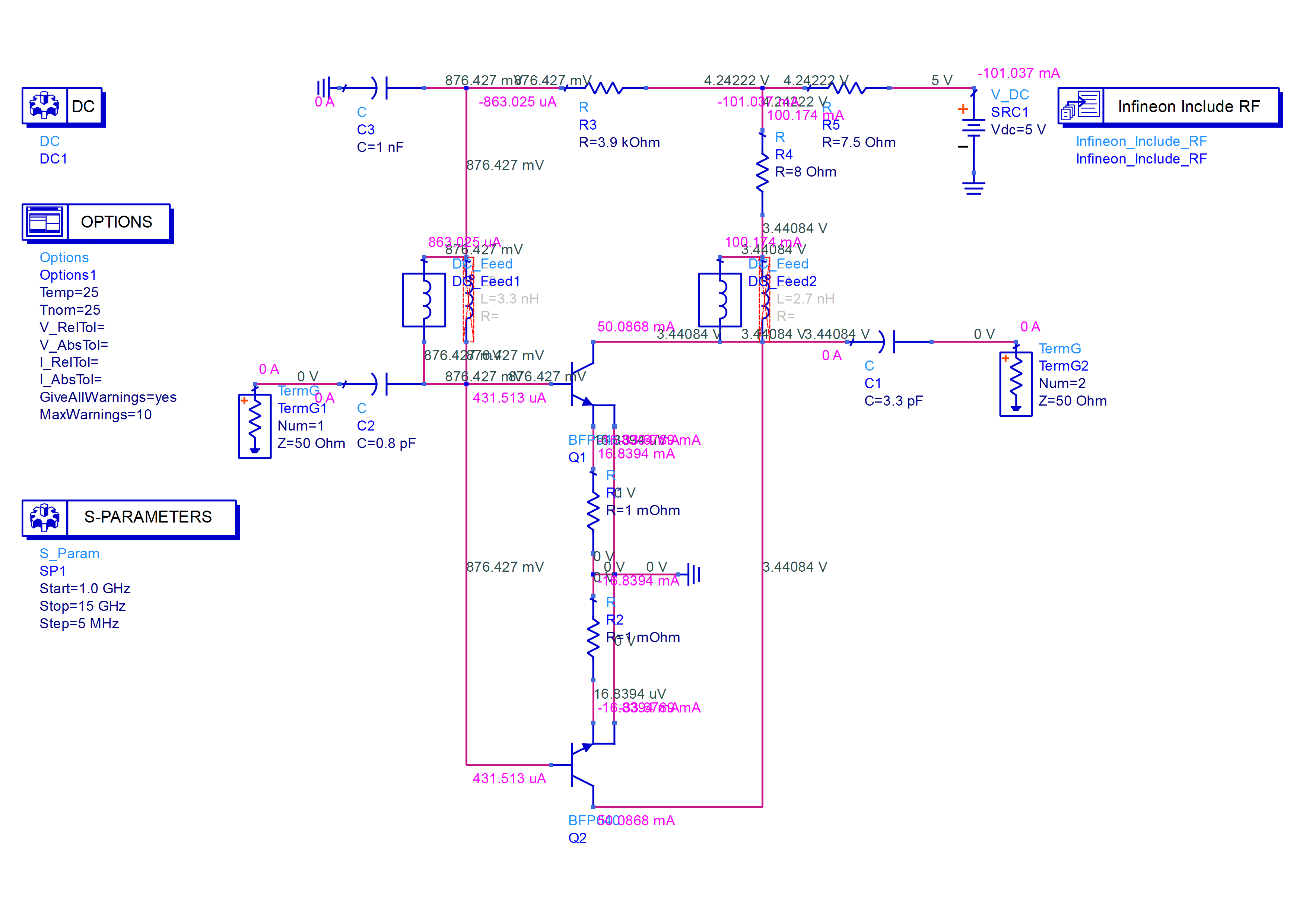
You use ideal capacitors and inductor in first figure.
You use DC_Feed and DC_Block in second figure.
Icc=101mA in first figure.
Icc=56.7mA in second figure.
They should be same.
5Volts - 56.7mA*7.5ohm = 4.57Volts.
However it is 2.17Volts in second figure.
Very strange.
Show me two ADS Netlists.
See https://www.edaboard.com/thread346180.html#2
(1) Netlist for first figure using ideal capacitor and inductor
(2) Netlist for second figure using DC_Block and DC_Feed.
You showed SPICE Netlist.
Show me ADS Netlist.
Why are these different ?
Options ResourceUsage=yes UseNutmegFormat=no EnableOptim=no TopDesignName="bfp640esd_lib:Schaltplan:schematic" DcopOutputNodeVoltages=yes DcopOutputPinCurrents=yes DcopOutputAllSweepPoints=no DcopOutputDcopType=4
#include "C:/Users/Stephan/Infineon_RF//circuit/models/RF.net"
C:C1  N__12 N__18 C=0.8 pF
C:C4  N__8 N__3 C=3.3 pF
C:C3  N__21 0 C=1 nF
C:C2  0 N__14 C=1 nF
L:L1  N__14 N__18 L=3.3 nH Noise=yes
L:L2  N__6 N__8 L=2.7 nH Noise=yes
R:R3  N__21 N__6 R=8 Ohm Noise=yes
R:R2  N__14 N__21 R=3.9 kOhm Noise=yes
R:R1  N__25 N__21 R=7.5 Ohm Noise=yes
BFP640:Q1  N__8 N__18 0 0
BFP640:Q2  N__8 N__18 0 0
V_Source:SRC1  N__25 0 Type="V_DC" Vdc=5 V SaveCurrent=1
Port:Term1  N__12 0 Num=1 Z=50 Ohm Noise=yes
Port:Term2  N__3 0 Num=2 Z=50 Ohm Noise=yes
S_Param:SP1 CalcS=yes CalcY=no CalcZ=no GroupDelayAperture=1e-4 FreqConversion=no FreqConversionPort=1 StatusLevel=2 CalcNoise=no SortNoise=0 BandwidthForNoise=1.0 Hz DevOpPtLevel=0 \
SweepVar="freq" SweepPlan="SP1_stim" OutputPlan="SP1_Output"

SweepPlan: SP1_stim Start=1.0 GHz Stop=15 GHz Step=50 MHz

OutputPlan:SP1_Output \
      Type="Output" \
      UseEquationNestLevel=yes \
      EquationNestLevel=2 \
      UseSavedEquationNestLevel=yes \
      SavedEquationNestLevel=2

#load "python","LinearCollapse"
Component Module="LinearCollapse" Type="ModelExtractor" NetworkRepresentation=2

Options ResourceUsage=yes UseNutmegFormat=no EnableOptim=no TopDesignName="bfp640esd_lib:Schaltplan_nur_Transistor:schematic" DcopOutputNodeVoltages=yes DcopOutputPinCurrents=yes DcopOutputAllSweepPoints=no DcopOutputDcopType=4
#include "C:/Users/Stephan/Infineon_RF//circuit/models/RF.net"
S_Param:SP1 CalcS=yes CalcY=no CalcZ=no GroupDelayAperture=1e-4 FreqConversion=no FreqConversionPort=1 StatusLevel=2 CalcNoise=no SortNoise=0 BandwidthForNoise=1.0 Hz DevOpPtLevel=0 \
SweepVar="freq" SweepPlan="SP1_stim" OutputPlan="SP1_Output"

SweepPlan: SP1_stim Start=1.0 GHz Stop=15 GHz Step=50 MHz

OutputPlan:SP1_Output \
      Type="Output" \
      UseEquationNestLevel=yes \
      EquationNestLevel=2 \
      UseSavedEquationNestLevel=yes \
      SavedEquationNestLevel=2

#load "python","LinearCollapse"
Component Module="LinearCollapse" Type="ModelExtractor" NetworkRepresentation=2
Port:Term1  N__12 0 Num=1 Z=50 Ohm Noise=yes
Short:DC_Feed2  N__14 N__18 Mode=-1
Short:DC_Feed1  N__16 N__8 Mode=-1
R:R3  N__21 N__16 R=8 Ohm Noise=yes
R:R2  N__14 N__21 R=3.9 kOhm Noise=yes
R:R1  N__25 N__21 R=7.5 Ohm Noise=yes
Short:DC_Block1  N__12 N__18 Mode=1
Short:DC_Block2  N__8 N__3 Mode=1
Port:Term2  N__3 0 Num=2 Z=50 Ohm Noise=yes
BFP640:Q1  N__8 N__18 0 0
BFP640:Q2  N__8 N__18 0 0
V_Source:SRC1  N__25 0 Type="V_DC" Vdc=5 V SaveCurrent=1
DC:DC1 StatusLevel=2 DevOpPtLevel=0 UseFiniteDiff=no PrintOpPoint=no Restart=1 \
OutputPlan="DC1_Output"

OutputPlan:DC1_Output \
      Type="Output" \
      UseNodeNestLevel=yes \
      NodeNestLevel=2 \
      UseEquationNestLevel=yes \
      EquationNestLevel=2 \
      UseSavedEquationNestLevel=yes \
      SavedEquationNestLevel=2 \
      UseDeviceCurrentNestLevel=no \
      DeviceCurrentNestLevel=0 \
      DeviceCurrentDeviceType="All" \
      DeviceCurrentSymSyntax=yes \
      UseCurrentNestLevel=yes \
      CurrentNestLevel=999 \
      UseDeviceVoltageNestLevel=no \
      DeviceVoltageNestLevel=0 \
      DeviceVoltageDeviceType="All"
There is no difference on my set-up

Here AWR results
Small_Signal.pdf
