Stray capacitance/inductance on CPWG
I have an RF PCB with CPWG that changes it's sizes.

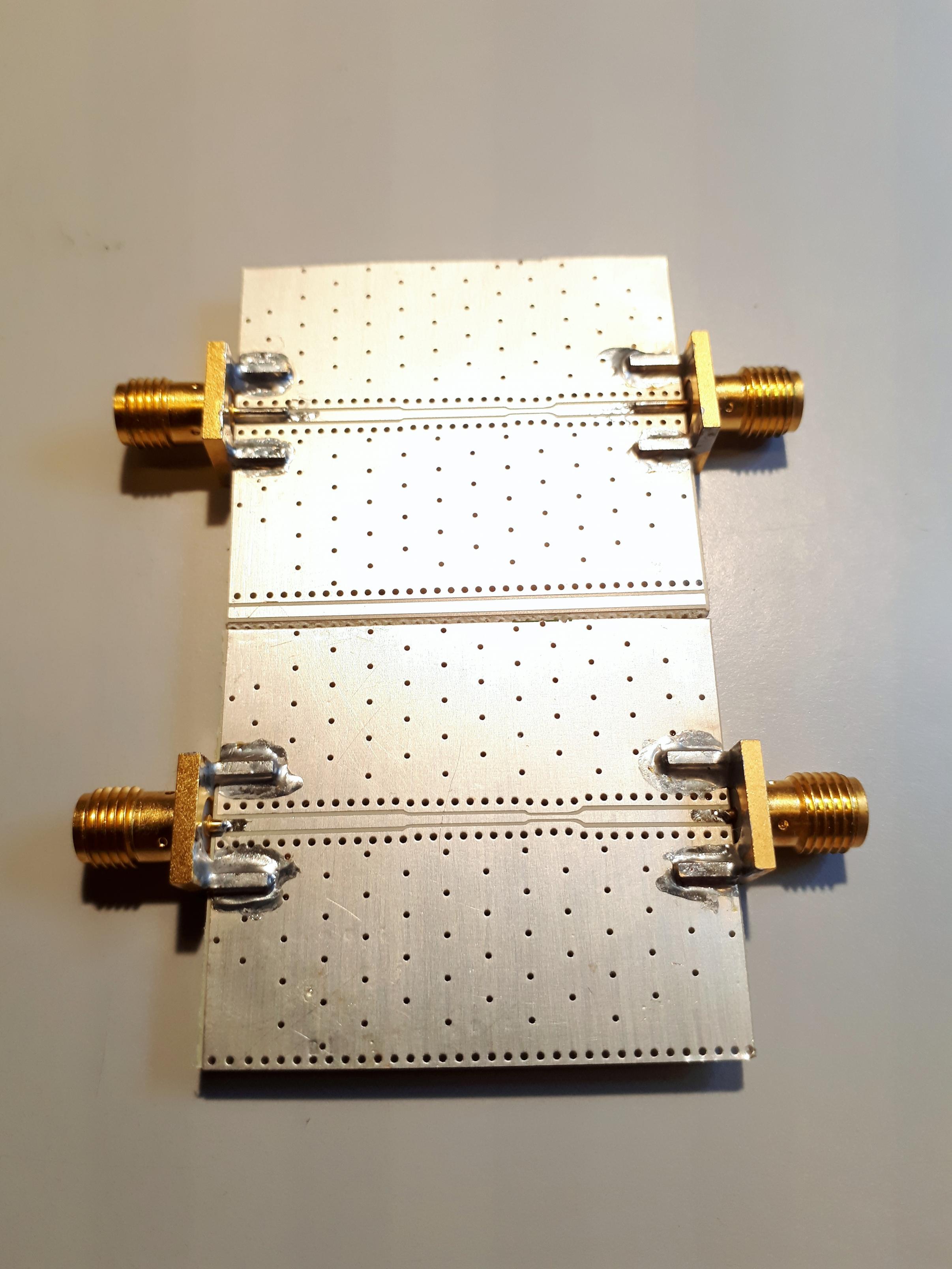
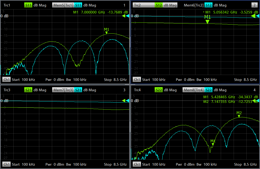
See the attached photo. I wanted to measure this board with a VNA. I first attached SMA connectors with long (4mm) central pins (the top PCB on the photo). The RL was not that great. I then thought that it is affected by stray capacitance of the very long pin and solder under it. I cut central pins to approx. 1mm and soldered them to another board (the bottom PCB on the photo). I see on VNA that RL is greatly improve.

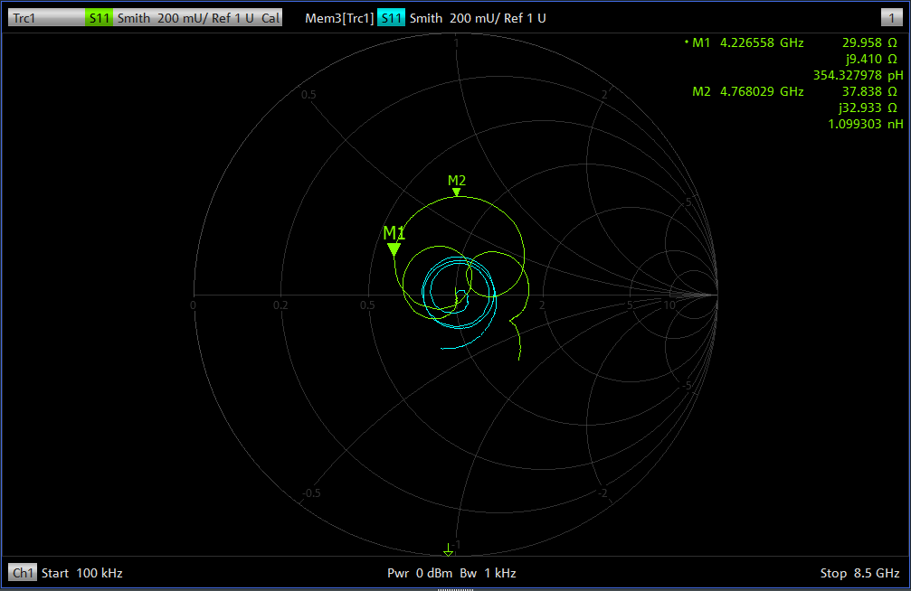
The green trace is for the SMA connectors with long central pins, the blue trace is for the SMA connectors with trimmed central pins. What puzzles me is that according to Smith chart, the long central pins and solder under them introduces more stray inductance rather than stray capacitance. I expected stray capacitance. Does anyone know why is that?
Thanks
The structure involves multiple λ delay. How can you know if the connector effect is inductive or capacitive?
Hi FvM,
Thank you for the reply.
Well, the longer pins have larger surface areas, hence the larger capacitance.
Do you mean that I have λ/4 rotations around the center of Smith chart that convert the stray capacitance to the stray inductance?
The Characteristic Impedance varies along the line.So,what you would expect rather than that ?
Your S11 plot shows the superimposition of two connectors and all the discontinuities along the line. A transformation into time domain (TDR display) can show the location of impedance discontinuities.
I agree with BigBoss, why are you using stepped transmission line width?
This is a test line. I am going to place three different components (IC, bypass cap and atten) on the same line. These components have different dimensions this is why the width and ground spacing of the CPWG changes along the line. I made this first board with EM simulation. The RL is 16dB. Will improve with the design.
I totally forgot that the physical length of the board is larger than the wavelength! My bad.
wow, with those junky connectors, you are not happy with 16 dB return loss?
You think that this connector https://eu.mouser.com/datasheet/2/70...0L5-779416.pdf is not appropriate for 8GHz application?
I made this board WITHOUT EM simulation.
As long as the back of the connector is tight up against the board, you are ok at 8GHz. Sometimes you have to run a bead of solder along the underside of the connector under the pin. Getting a good ground on board edge connectors is easy, after being burnt a few times.
-Which substrate you have been using for 4GHz ? Characteristics ?
-If you supply Gerber file, I can simulate it for you to compare the results if you desire.
-What is your intention by changing line width ? A special case ?
I used RO3006.
I have actually simulated the board last week. The simulated and measured S-parameters are quite similar. The reason why I changed the line width is because I am going to mount different RF components on one CPWG. These components have different dimensions.
If you intend to mount some SMD components, there is no sense to talk about the Characteristic Impedance of the Transmission Line.It will show somehow discontinuities along the line and each node will have different impedance value.
The stepped line width it going to make extracting the properties of components soldered along the line quite difficult. The same will apply to parasitics in the line itself. You're just making things difficult for yourself.
In my application, RL is quite critical. I made this test line to see what RL to expect. For example, I found out that an attenuator that I was going to use, doesn't work well with CPWG. Say, I get 16dB RL with only the transmission line. I installed 3dB attenuator and instead of getting RL 22 dB I got RL 14 dB!
Are you sure that the used chip resistors are suitable for 8 GHz? CPGW as such shouldn't be a problem with sufficient fine via fence. I would also prefer symmetrical shunt elements. Did you try to model the chip parasitics?
Do you mind to show a photo of the attenuator setup?
The attenuator I was going to use is this one https://www.digikey.dk/product-detai...23CT-ND/948902
VSWR <1.2 up to 20GHz

This is little bit different CPWG. The S-parameters

The blue traces are S-parameters of the CPWG with installed connectors. The green traces are S-parameters after I cut the CPWG and placed the attenuator.
The reason for such a bad RL is that this attenuator doesn't work well with CPWG. It was designed for usage with microstripes.
0805 size attenuators will have this type of return loss. It has little to do with coplanar/microstrip. If you flip the chip, you will get a little more bandwidth/return loss out of it... but will handle less power. Company called IMS Resistor has better (more honest) documentation on performance. (I do not work for IMS).
Your test is invalid. This math would only apply if you place the attenuator directly at the line input (to exclude mismatch of the line itself) and the coax to microstrip transition itself is perfect.
capacitance Stray CPWG 相关文章:
- How to take ESD and pad capacitances into consideration during design
- Re: Calculate Capacitance Value from Smith Chart
- Calculate Capacitance Value from Smith Chart
- How the capacitance varies as input power varies in a mmW RFIC PA?
- How does the capacitance of a patch antenna affect its resonance frequency
- Calculate capacitance on SRR
