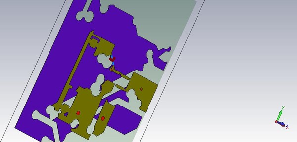
a problem on a ground impedance analysis of pcb
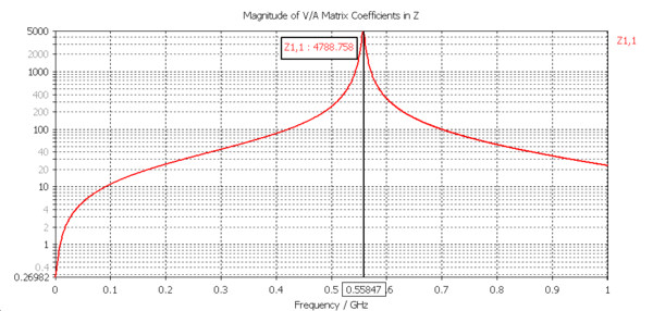
the impedance is big at 558mhz, the electric size is smaller then 558Mhz.
I'm a newer in RF,anyone can tell me what reason can cause this and which theroy can explain it.
thanks a lot


Hi,
Is blue your GNd or what, & what are dimensions pls?
K.
both are gnd
the attachment is my model which is igs format
Hi,
for me is a basic problem to see: nothing is RF proof here!
Itself the better blue-layer is not enough good for low impedance (RF) GND!
You have to eliminate the lot of cut-ins/channelyzings, and as I can it see, the green layer has only 4 contacts to the blue, and is realized as a collection of wider lines (others sayed: inductances)_ nowhere is a plane to find. (I dont open your modell)
Sorry, but not a wonder if your resonance is at 5-600MHz...
K
thanks for your reply
this is a RI problem ,the gnd is poor trully,we have fix it by modify gnd
but my boss ask me to find the theroy back why it is sensitive to a Interphone which work at 430MHZ
Yes,
its very poore as RF GND...
Your system must be sensitive for the most frequencies over so 100(+/-50) MHz.
Check pls your impedance plot; at 430MHz it has an impedance of ca. 100-150 Ohm, also so ca. 100x higher as a GND has to have...
I think, it has problems in the full UHF/VHF band_in so 200...800MHz range.
You must have a full plane as GND, than the second layer can be connected over some via`s (short as possible), but make pls not so an "sloted" structure, these is a collection of different (and mostly coupled with the next one) resonators, but hes behavior is minimum inductive dominant, what you can not need too.
You can have some "preparation" for the GND quality if you apply a shield case, or minimum small metallic wall around, over that, but the best solution is a good designed GND-Layer(full plane), even if its multilayer!
K.
I think i get what i want from your reply
thanks a lot , K
Hi flatcloud,
You are welcome!
Let know pls what will be your progress...
Greetings!
Karesz
Hi K.
I have fixed my problem
the gnd is an osc gnd of mcu,the mcu doesn't work in worse RF Environment, I find when rf Interference on,the wave of osc is very poor even no osc wave , i modify the gnd,then it is fixed,so i want to find why and do not make the same mistake. Minimum opening slot is the best solution
thanks for you help , K
Hi!
Your welcome!
For good RF performances we have every time GND & supply coppers as a plain (or minimum very wide coopers for supplying potentials, but GND ever as a plain) to realize!
Plains are (if only possible) not to mix with other potencials/signals (danger of making slotes)...
If you have on two_or more_ layers GND (supply too) checck pls, that they are with much as possible THICKER Vias/holes (as the general versions) contacted to the base layer (you can see so a technic on good RF/UHF PWR amplifyer PCBs ...
Good progress!
Karesz
Hi
I think reduce slots on gnd is the point
I have made a simulation,It is true
I maked never a GND simulation, but some Highspeed/High complexity PCBs and usually their are as first version approbed.
OK, I know nothing is 100% sure in life, but lot of behaviors are predictable...
K.
