waveguides in cut-off are not matched !!!
3D EM simulations from waveguides in cut-off, e.g. a transition from microstrip line to hollow waveguide, always show well matched conditions at the cut-off waveguide port. In fact, there should be great reflection.
Somebody interested in commenting ...
-e
this "cuttoff waveguide port" is placed many wavelengths down the waveguide?
Well, it doesn't matter if the cut-off waveguide port is placed lambda/2 or 100*lambda from the transition.
In all cases, S11 is matched.
The question is, what type of 2D EM field is impressed at the hollow waveguide at low frequencies ?
Even if it is the "right" 2D field, that corresponds to the evanescent mode. If it carries 1 Watt of RF power, nearly none of this power is dissipated but nearly all of this power is reflected (in the real world).
Considering the fact that the reactive near field of a cutoff waveguide (or antenna) really never extends past about lambda/4 in field strength, your result does not surprise me. So if you have a port that is in cutoff that is located lambda/4 from the T-Line transition, the transmitted field immediately begins to decay, reaches the discontinuity and reflects... but the reflected field will continue to decay on its way back to the port of measurement for a total distance of travel of lambda/2. Since all the fields decayed substantially prior to returning to the transmitting port there are no perceived reflections measured at the transmitting port so the S11 will look very well matched as all energy was attenuated in the structure. If you wish to see what you seem to be looking for, you will need to place the port much closer to the discontinuity (less than lambda/8). Even then, you will likely need to overmode the transmitting port as there may be many evanescent modes excited by the spurious reflection at the T-line discontinuity.
Long Story Short: It is never as simple as it appears, and, in general, EM tools accurately represent the physics (we just misunderstand the physics at times ;))
Have Fun
Are you talking about the return loss of a waveguide port below cutoff frequency?
From my simulator, I get total reflection below cutoff frequency, as expected.
That would not be true. If you put a mathematical port at the start of the cuttoff waveguide, then you will have a good match. If you put the mathematical port after some length of cuttoff waveguide, say 4 wavelengths, then I would expect S11 to be 1. It takes many wavelengths of cuttoff waveguide for the evanescent modes to die down.
you should only get a total reflection if you are matching to a real impedance as a reference (expecting a propagating mode) This is why measurements always show total reflection as the cutoff waveguide must be fed by a propagating feed which is the [real] reference. If you use generalized S parameters that are complex conjugate matched (Circuit definition), rather than real matched S Parameters (which is the RF definition of S parameters) then one would have no reflections... It is a bit of nomenclature, but the difference between a real reference S Parameter and Complex Conjugate matched S Parameter is the main difference in what S11 is simulated to be.
Have Fun :)
Hello, thank you for your comments.
Finally, I agree with tallface. The 3D EM simulation tool excites a decaying (evanescent) mode at the cut-off waveguide port. This mode does not entirely reflect, but comes back to the port with a power level, lets say 40 dB below the input power level. Anyway, it is not possible to establish this scenario in an experiment, because we cannot PURELY excite the evanescent mode. In the real world, the RF power from a signal generator is coupled to the cut-off waveguide by an appropriate structure. This structure does reflect back nearly all of the input power (S11=0dB). Otherwise attenuators could be built utilizing cut-off waveguides, and this is not possible.
--- just for the record -- I dont agree with your "conjugate match" argument. In fact, the generalized scattering parameters from 3D EM simulators belong to the traveling-wave scattering parameter calculus (see http://www.eeel.nist.gov/dylan_paper...cuitTheory.pdf)
-e
- - - Updated - - -
at volker muehlhaus: Sonnet EM does always use waveguide ports (lumped ports, discrete ports) with defined reference impedance. This 2.5D EM tool cannot excite the pure evanescent mode.
For this 3D model with waveguides, I used the Empire XCcell 3D FDTD simulator:

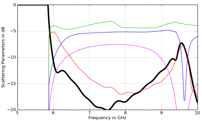
at volker_muehlhaus: Ahh, ok. You use a real 3D EM simulation tool. I cant see it in the picture - is the excited port at cut-off or do you simulate a transition from circular wavguide to cut-off waveguide ? The latter case shoudl show reflective behaviour (S11=0dB) as your result plot does.
The green port is excited at 5 GHz, which is below cutoff (5.855 GHz). You can see the fields decay in the first screenshot, and you can see S11=0dB (black curve) and very small S21,S31 in the second plot.
Hello Volker,
I have tried a similar setup with our 3D FEM EM simulation tool.
In case of generalized scattering paramters (not renormalized to a fixed ref. imp.) the cut-off waveguide shows matched behaviour.
Renormalization leads to your results.
Thanks again...
-e