Re: A problem in frabrication: Narrow band filters
Regarding the CST settings: I am not a CST user, so I am not sure if these settings are complete. Maybe someone else can comment.
With the metal thickness, the 1.75μm look wrong and should be 17.5μm.
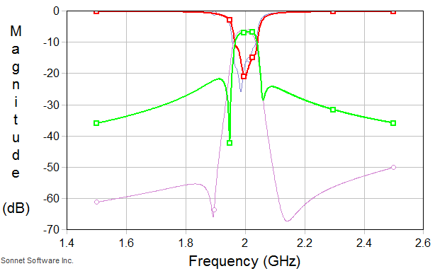
That Ripple in your "Measured S21" (Black Trace) looks like you have a bad
Cable/cal. Make sure the cables are all tight and re-Cal. You SMA connectors could
be better.
1) Eliminate that air Gap
2) Trim the center pin of the SMA (that touches the PCB).
3) if you can cut the center pin to slope down towards the PCB, Having a smooth
Transition is better.
4) Make the solder smooth and as thin as possible.
In my opinion CST is not the easiest tool to simulate this kind of filters. I would be better use a palanar simulatore like sonnet, or emsight.
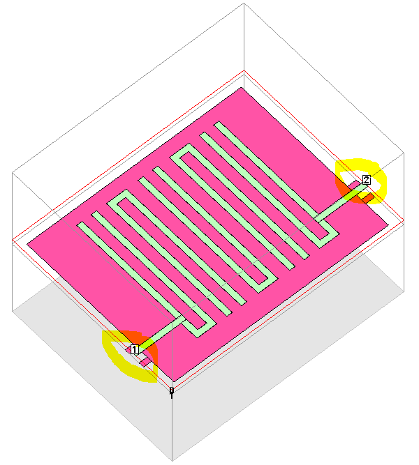
Again in my opinion the right disign procedure for this kind of circuits is: design the filter with the linear simulator, make a yeald analisys respect the fabrication tolerances and then check the design with the EM simulator. Another important thing is to take care about the measurement: If you design and the EM simulate a filter inside a box, you must test the prototipe in the same box.
Ciao.