Using Manufacturer S-Parameter data - question.. 2 to 20GHz
时间:03-30
整理:3721RD
点击:
When we get a set of S-Parameters for a device, say from a .s2p file, or from a design kit, we hope they were measured with a test jig, "zeroed out", such that the mounting kit and test jig itself does not contribute to the data, right up to the "reference planes".
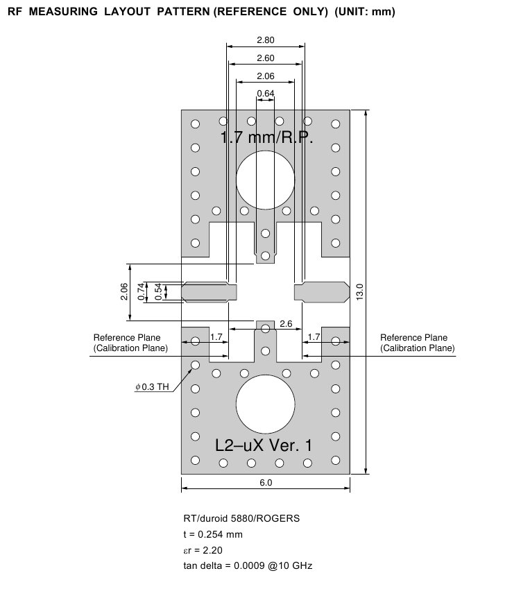
We also find a "Reference Measuring Layout" in the datasheet.
Here is an example for a HJ-FET:
The gate is to the left, drain to the right, and there are two source connections, one each at top and bottom.
This layout probably would not be simply imported into a final design - it includes a couple of large fixing holes.
So some questions..
Would the published S-Parameters include an assumption that the layout shown has such a good grounding at the sources that the impedance at the sources is too low to matter? ie. Does the published S-Parameter set include the measuring layout characteristic "built-in" ?
Alternatively, can we assume the effect of the reference measuring layout has been eliminated right up to reference planes at the grounded source connections? The diagram only shows reference planes on the gate and drain. This unsettles me. Why do we need the measure layout anyway?
My reason for asking is that an EM simulation of a source connection on that reference layout shows enough impedances to care about, given that I would like to include a little inductance of my own in the source connections. The amount needed is very little, being made only in the inductance of some grounding vias at the sources, but essential to stability. I need to find out what is the norm here - when it comes to S-Parameter data.
We also find a "Reference Measuring Layout" in the datasheet.
Here is an example for a HJ-FET:

The gate is to the left, drain to the right, and there are two source connections, one each at top and bottom.
This layout probably would not be simply imported into a final design - it includes a couple of large fixing holes.
So some questions..
Would the published S-Parameters include an assumption that the layout shown has such a good grounding at the sources that the impedance at the sources is too low to matter? ie. Does the published S-Parameter set include the measuring layout characteristic "built-in" ?
Alternatively, can we assume the effect of the reference measuring layout has been eliminated right up to reference planes at the grounded source connections? The diagram only shows reference planes on the gate and drain. This unsettles me. Why do we need the measure layout anyway?
My reason for asking is that an EM simulation of a source connection on that reference layout shows enough impedances to care about, given that I would like to include a little inductance of my own in the source connections. The amount needed is very little, being made only in the inductance of some grounding vias at the sources, but essential to stability. I need to find out what is the norm here - when it comes to S-Parameter data.
Typically the S-Par's are just the IC (all connector/jigs are De-embedded).
The Test jig is typically what the Manufacturer uses to get the performance
that they describe in their data sheet.
Many thanks for the reply. I know that some folk have access to kit so they can measure (and even select!) devices for themselves, but I am one of those who has to rely on the vendor data.
I needed to be sure that vias and tracking I put on the source connection would have the effect I intended.
G
