Substrate definition of transformer
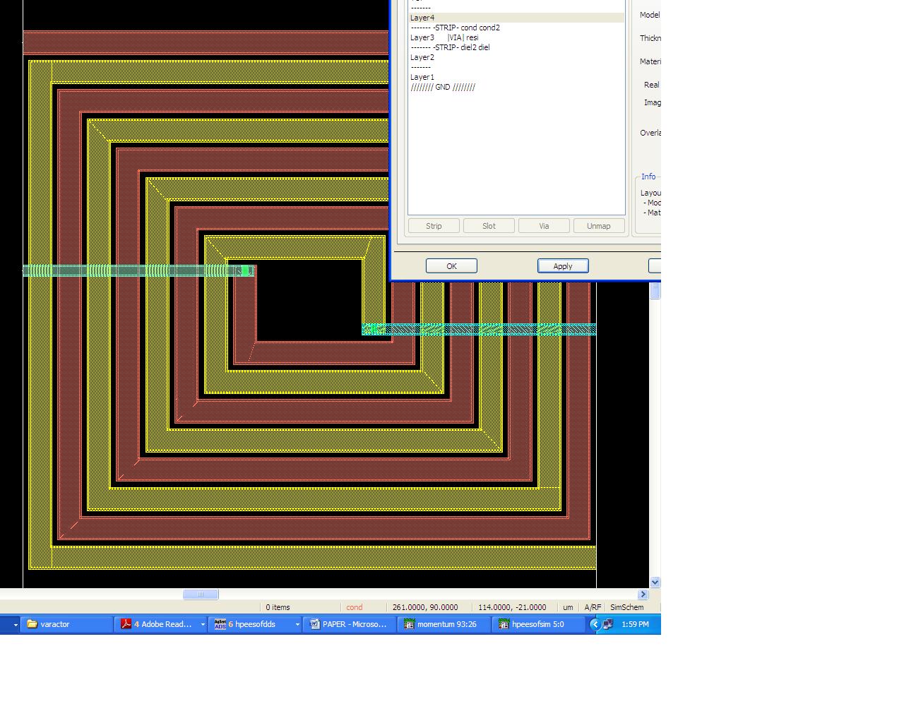
I am designing transformer. I follow the substrate definition of inductor on silicon
Top
-------- Strip -cond2
layer3 Via |resi|
-------- Strip cond
Layer2
---------
Layer1
//////GND//////
For transformer design , I have to use two different metal lines
Top
-------- Strip -cond2 cond
layer2 Via |resi| |hole|
-------- Strip diel2 diel
Layer1
//////GND/////
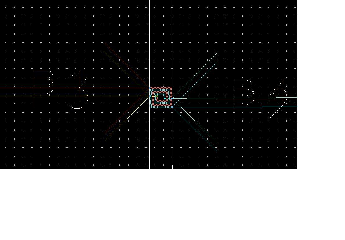
Is it correct sir? T I hereby attached the example design. Please see and tell your suggestion for transformer design.Please help me .
Urgent
What is your top? Air? I think you should add some substrate above cond2. I can't see your example. Software is ADS momentum?. Your stack-up for transformer design: Why you use two layers (resi and hole) for via definition?
Maybe some example:
Top [AIR]
subst
-------- Strip
subst Via
-------- Strip
subst
---------
Si
//////GND//////
Hi,
Thanks. Now I used one layer for via and two layers for metals and underpasses.See my design

Maybe post again your stack-up because a layer for vias seems not to be correct, it should be inside the substrate layer.
Hi,
I couldnt understand. I think , i incorporate your comments. Please see my design . Where i made wrong? Please correct it.

Ah ok, seems to be correct now.
Hi, What is the purpose of take layer 1 and layer 4 here? Is it to confine the fields around the inductor structure?
I dont know. I have seen some examples in ADS so I put.
Yes u r correct. Ill remove layer 1 and 4. Otherwise the design is ok.
Is it a transformer that u r trying to simulate or just an inductor? Clearly the structure is an spiral inductor, and Planar transformers are totally different having cores and etc.. ?
i am trying mutual coupled inductors . Please explain where it is wrong?
