how to set lumped Port reference for pad bump simulation in HFSS
时间:03-30
整理:3721RD
点击:
Hi
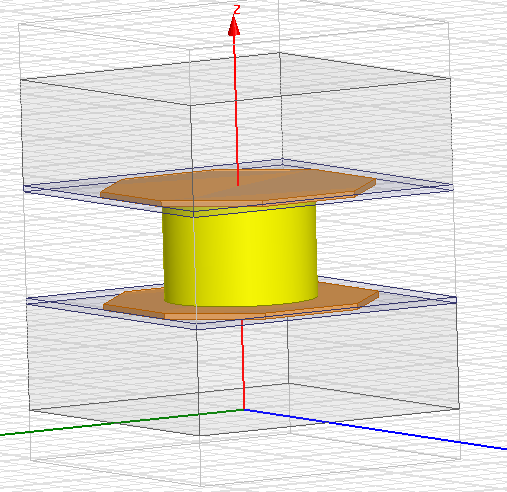
Can anybody help to explain how to assign excitation for this two pads, basically i want to simulate the flip-chip bump.
I have assigned ground plane at the top and bottom faces of the dielectric materials. but they are not touching the bottom face of the bottom pad and the top face of the top pad, respectively. so when i was trying to add lumped port for the pads, there has no reference plane for me to choose.
Thanks!
i read from the manual "an introduction to HFSS". but i still don't know how to do it after reading