[ADS] generating layout from schematics
Did you specified your substrate with MSUB? Place a picture of your MSUB and MLIN definitions please for further help.
Did you also use the proper MTEE, MBEND, MCROSS or just straight lines?
dear DR volker,
thanks for the question.
i just replace with straight lines only. meaning MLIN only. no MTEE, MBEND or MCROSS.
hi Ascozes,
attached pictures here with questions.
i have few questions:
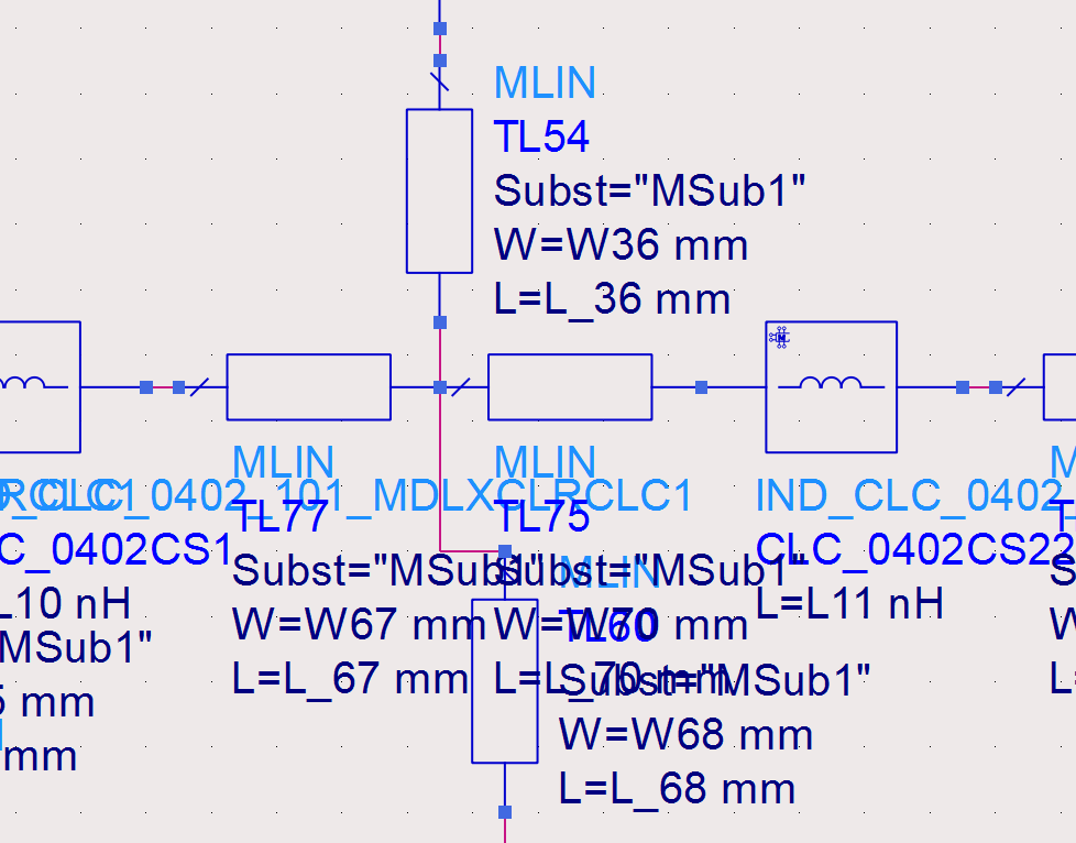
1) please look at the picture below. its looks like a cross. what type of "TLines-Microstrip" i should use here?
2) i replaced terms with port and used MLIN to interconnect between components. Am i correct here?
3) the gate of the device has DC and RF interconnect together. what type of "TLines-Microstrip" i should use here?
4) please refer to the same pic in question 3). how can i connect ground that way as shown in the picture. thanks for the answers in advance.
MCROSS for cross junction
Sounds ok.
MTEE for T junction.
Just have a look at the microstrip element palette and you will see more. For example MBEND for 90° corners.
Dear Dr Volker,
i will try out your suggestions and update the progress by end of today. thanks alot for the inputs.
Dear Dr Volker,
i have tried as per your suggestion. now i can see almost the complete layout there but its abit messy because few structure stacked on top of each other. i think i need to have enough space between those structure to avoid this issue. please give me your suggestion.
apart from that, im getting below warning for active devices. is that means layout footprint not available for these devices? im using modelithics library.
Failed to setup expression context to generate parameterized design.
Cannot push into primitive instance "INF_BFP420_4" on design "xxx:layout".
Failed to setup expression context to generate parameterized design.
Cannot push into primitive instance "AGT_ATF54143_2" on design "xxx:layout".
Failed to setup expression context to generate parameterized design.
dear dr volker,
i have few more questions here.
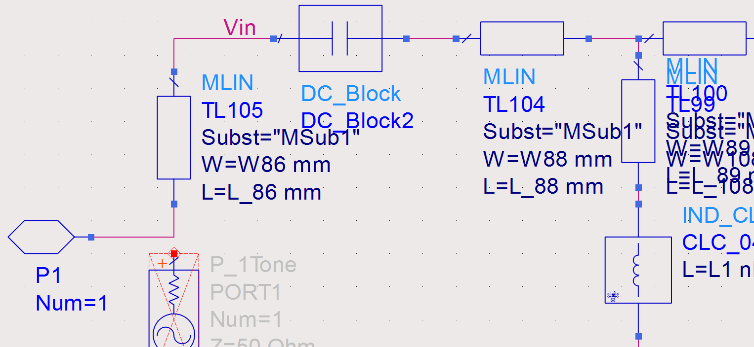
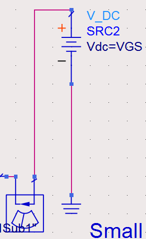
1) i have component such as current probe and DC supply in the schematic. am i suppose to remove them before generating layout? does layout generated for DC supply as well?
2) i did connect a MLIN from DC power supply to ground as shown in the pic below.
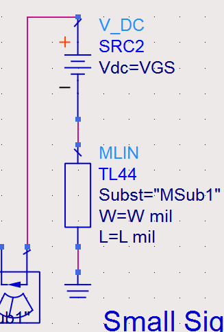
however, when the layout is generated, TL44 is separated from the rest of the layout so i removed TL44 from the schematics as shown in pic below.
3) one of my friend suggested this. "Schematic to layout can sometimes be rather iffy if you auto-generate it.* You may have to "pick & place" items from the schematic to layout manually.* In the schematic window, somewhere*within the menus there should be a "place from schematic to layout" option.* You will need to enable snap to pins in layout so your layout elements will snap pin-to-pin.* Also, make sure they are on the same layer, eg COND1"
i think he suggesting to use Layout --> place component from sche to layout instead of Layout --> Generate/update layout. what is your opinion. my circuit is large and complex. what method is recommended for my design. im getting different results for these two methods. thanks in advance.
Not sure how to help you ... if you need extra spacing, create it by adding/changing microstrip elements.
I don't know. Modelithics library usually has layout. "Expression context" sounds like a different problem, so maybe Modelithics support can help you.
You can you move the source to the end (at the GND symbol). Then you don't need a layout element for the source.
Your friend recommends a good method, because then you place elements in layout step by step. This can be easier than placing all at once from schematic.
dr volker,
thanks for your comments. im currently working on my layout. its not perfect yet but im hopeful to get it right. i have one more question.
can we do multilayer PCB using ADS generate/update layout? if yes, could you please tell me how?
Too much detail to write it in a forum post, but there might be some documents by Keysight, or even in the online help. The idea is that you can set layout layers for elements in the MSUB block. You can also have multiple MSUB blocks, and configure in the microstrip models which MSUB (-> set of layers) you want to use.
dear dr volker,
i tried searching examples but its only available for basic problem. its not available for complicated problems like mine. even ADS cook book doesn't have it.
if you have any examples to Auto create multilayer PCB in ADS, please share here. it will be really helpful.
dear volker,
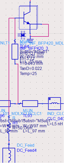
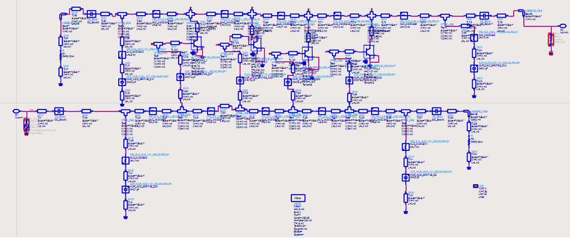
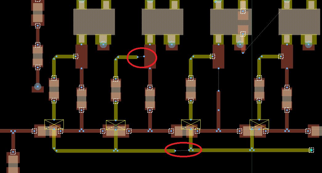
i have another question. im creating layout for my distributed PA. but its looks weird! please refer to pics below.

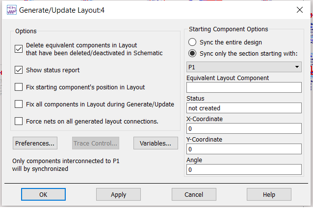
this my generate/update layout window before i click apply/ok
actually this is not my full circuit. its part of it only! i even removed DC biasing from the circuit to see if it can generate the layout properly. but it still couldn't
the problem is gate artificial transmission line disconnected from the device!
It looks like some paths take the wrong direction. You need to check manually where that happens. And there are many nodes that look unconnected (with the light blue diamond symbol).
I can't tell you an easy way to auto-generate this layout. It is a lot of work.
20 years ago I created such schematic-to-layout software (sold through Ansoft) and understand what you want, but it's not fully automatic.
dear dr volker,
i clearly understand now that its not fully automatic. all i want is ways to troubleshoot my problems. my questions are:
1)
can you pin point in the schematic where it took wrong direction? (its because im not able to figure out myself!)
2)
those node are connected in schematics. why its appear to be disconnected in layout? how to fix that based on your experience?
3) if you have answer for my above Quote, please help to share as well. thanks
Dr volker,
im able to figure it myself what went wrong. im progressing to generate multilayer PCB now. thanks for the guidance so far. i will post here my future problems.
i have another question. how to convert ground component in schematic to layout ground? when i use "generate/update layout", the ground component appears in the layout as well which is not true!

figure 1: schematic ground
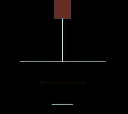
figure 2: layout ground
its suppose to connects to board ground thru a via..
Yes. Use a VIA element in the schematic instead of the ground symbol.
dear dr volker,
1) if i want to add more vias, i just more via connection to one node. is that true?
2) MSUB only gives us one layer (T and H). is there any component to define for multilayer board?
3) how to draw ground on top layer for microstrip line? is there any component for that in schematic?
4) please see figure below. is there any option to auto adjust the length of MLIN to connect automaticly? i designed RF line length on TOP layer and those are DC line length at the bottom
i have registered to keysight website and read "schematic_capture_and_layout" pdf. none of the useful information which you are giving listed there!
Yes, you can do that.
If you want to EM-simulate it and don't need an accurate electrical model from schematic, you can define another MSUB and map other layers in that MSUB. Than all elements using that second MSUB will draw on the layers defined there.
In the ADS forum, I saw that ADS also has elements for grounded coplanar. I have never used them, because my work ist mostly EM (not schematic).
No, unfortunately. You can use <Ctrl> + M to measure the required distance.
Thank you!
im using microstrip and not coplanar. what im looking for is ground separation between micro strip runners. please help.
how if i need accurate electrical model from schematic?
generating ADS schematics 相关文章: