求教后端初步布局过程第一步IO单元排布位置颠倒原因
用icc第一步创建了库之后,读入dc综合出的网表,然后读入IO单元放置文件(主要是pad_pad_physical_contraints 命令等);
从gui看到IO单元pin放置完全颠倒,见附图(红色线表示pin),本来应该是带有terminal的port置外;
我觉得我的库生成没有问题,因为参照Milkyway userguide,加入了tech lef,cell lef,以及lef mapping;
问题:是什么原因导致这些IO单元都颠倒了,放反了,虽然rotate 180可以解决?
谢谢指导!
附图上传没成功,在此补上
看下底部的IO是怎么放到,试试放IO的其他选项,实在不行就用手改下,然后存到def里面,以后就直接read def
IO单元放置文件应该可以定义IO的方向的,多看看UG
谢谢两位的回复!
IO单元上下左右都是反的,截的图只是我顶部反的一部分;
存到def文件里面然后更改def这种方法可行,但我想搞清楚为什么直接读自己生成的FRAM就反了,而IO工艺那边提供的库解压后的FRAM view读入正常;
至于IO放置确实有个选项可以更改IO方向,这个选项是set_pad_physical_constraint的-lib_cell -lib_cell_orientation但是这种改法导致给出pad limited;
以下是我的terminal结果和生产版图截图
terminal 运行部分结果:
Place pads/pins successfully
Increase Bottom/Top to core distance by 0.4
Pad Limited detected in Left/Right sides.
Enlarge core height to 10635.4 by 0.82
Core aspect ratio adjusted to 0.982
Core Utilization adjusted to 0.051
Pad limited detected. Try fixed die size floor plan ...
Start to create wire tracks ...
Start to place pads/pins ...
Information: The orientation of Library cell "PX3" is "N". (APLUI-043)
Information: The orientation of Library cell "PB12" is "N". (APLUI-043)
Information: The orientation of Library cell "POT12" is "N". (APLUI-043)
Information: The orientation of Library cell "PO12" is "N". (APLUI-043)
Information: The orientation of Library cell "PI" is "N". (APLUI-043)
Information: The orientation of Library cell "PISD" is "N". (APLUI-043)
Information: The orientation of Library cell "PISU" is "N". (APLUI-043)
Information: The orientation of Library cell "PCORNER" is "N". (APLUI-043)
Information: The orientation of Library cell "PVSS2" is "N". (APLUI-043)
Information: The orientation of Library cell "PVDD2" is "N". (APLUI-043)
Information: The orientation of Library cell "PVSS1" is "N". (APLUI-043)
Information: The orientation of Library cell "PVDD1" is "N". (APLUI-043)
Information: The orientation of Library cell "PVDD1CE" is "N". (APLUI-043)
Information: The orientation of Library cell "PDIODE8" is "N". (APLUI-043)
Information: The orientation of Library cell "PVDD1CAP" is "N". (APLUI-043)
Information: The orientation of Library cell "PVSS1CAP" is "N". (APLUI-043)
Information: The orientation of Library cell "PVDD1AP" is "N". (APLUI-043)
Information: The orientation of Library cell "PVSS1AP" is "N". (APLUI-043)
Information: The orientation of Library cell "PVDD5AP" is "N". (APLUI-043)
Information: The orientation of Library cell "PVSS5AP" is "N". (APLUI-043)
There are 0 pads constrained by min IO spacing.
Top core spacing increased, pad limited.
...
这是关于顶部放置完后的给出的结果,红色就是我上面说得pad limited情况
版图截图:
tcl部分脚本:
set_pad_physical_constraints-pad_name "PX3"-lib_cell -lib_cell_orientation { E E E E }
set_pad_physical_constraints-pad_name "PB12"-lib_cell -lib_cell_orientation { E E E E }
set_pad_physical_constraints-pad_name "POT12"-lib_cell -lib_cell_orientation { E E E E }
...
版图截图:
版图截图(继那个版图左侧局部,可以看到修正了IO单元pin的方向):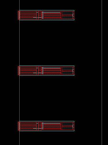
好大啊...
请问小编问题解决了吗?我也遇到这个问题了。
你是用Milkyway做的fram view吧。
如果是的话,可以试试在生成IO的milkyway中用GUI命令load clf(without timing information)来读一个clf文件。文件内容举例如下。
definePad "*" "180"
对,这应该是mw 做的问题,
第一步就卡住了》》》》
谢谢!
正在研究!
麻竹学习
同意,不过我们一般设270