Hspice学习帖
鉴于大家对Hspice的兴趣,特开此帖,方便Hspice新人学习。
费话不说,先帖网表。
---------------------------------------------
* Stripline circuit
*号开头为注释
*瞬态分析 从50ps到7.5ns之间
.Tran 50ps 7.5ns
*.OPTION 分析选项,用于定义模式精度等。
.OPTION post Probe
*V 开头为电压源 节点为1 0
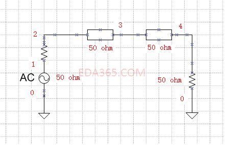
VIN 1 0 PWL 0 0v 250ps 0v 350ps 3.3v
*R 开头电阻 此处为电源内阻,节点为1 0
Rsource 1 2 50
*T 开头为无损传输线,节点为2 0 3 0
Tfirst 2 0 3 0 ZO=50 TD=0.17ns
*C2 3 0 2p
*T 开头为无损传输线,节点为3 0 4 0
Tsecond 3 0 4 0 ZO=50 TD=500ps
*此处为负载电阻,节点为 4 0
Rtermination 4 0 50
*查看1 2 3 4 点波形
.Probe v(1) v(2) v(3) v(4)
.End
可拷贝上述文字到文本文件,修改为*.SP文件,即可仿真。
------------------------------------
Hspice 软件下载地址:http://www.eda365.com/viewthread.php?tid=2779&highlight=hspice
大家有问题可在此处帖处,已供后来人参考。
1.电路图,方便理解网表
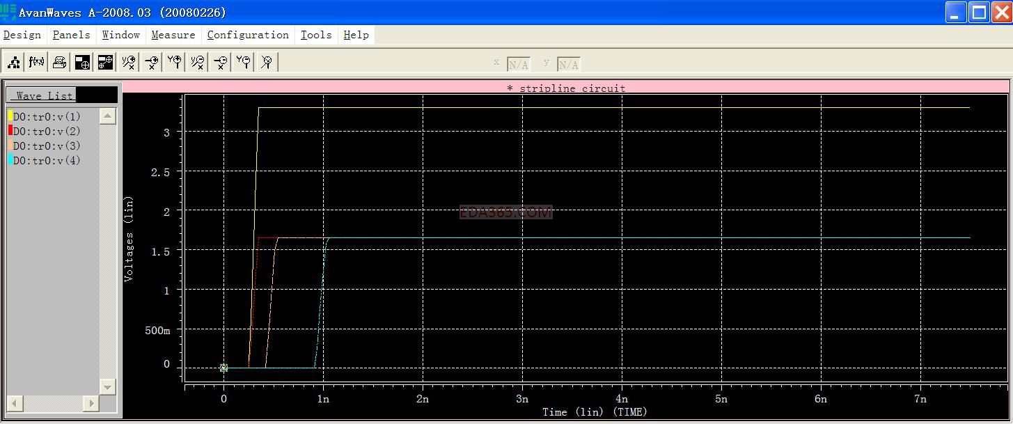
2.仿真波形图,由于完美阻抗匹配及无损传输线,所以波形比较漂亮。---图片单击可放大
此帖对于新手的确很受用
恭迎斑竹继续补充
很有帮助,以后经常来学习
下个内容参数扫描分析。
第二讲。
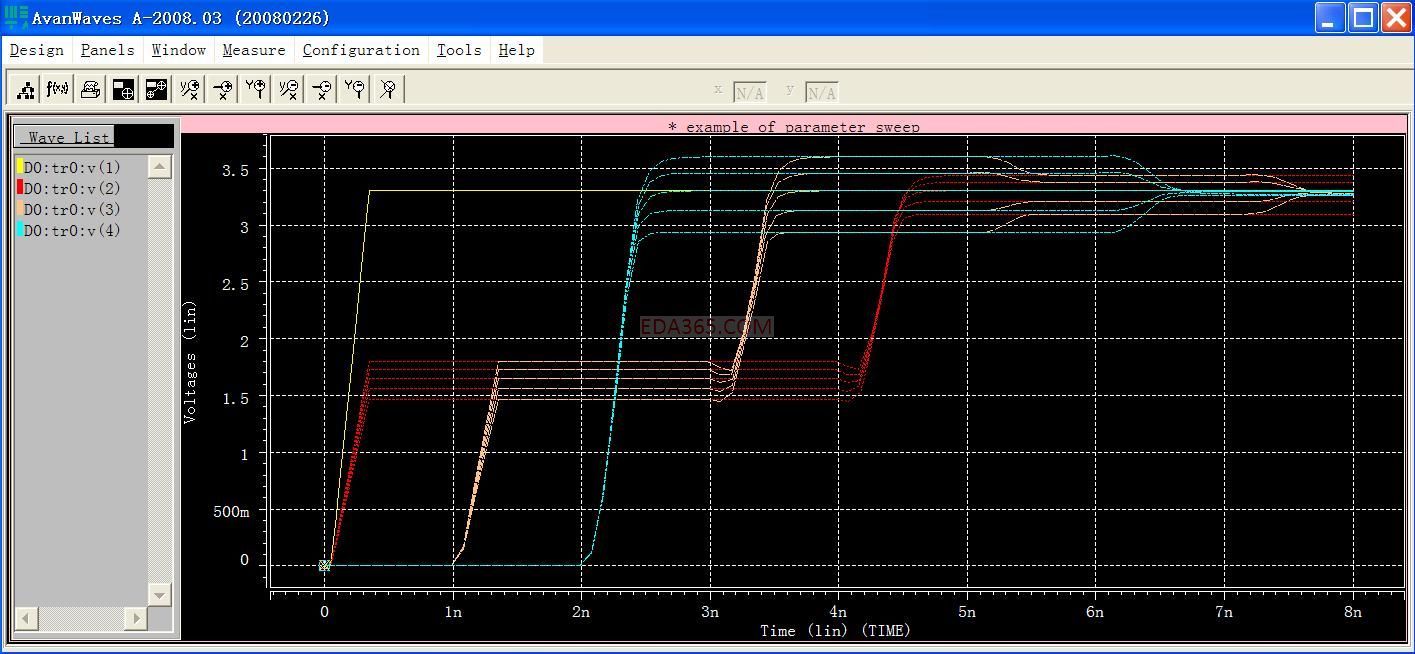
1.参数扫描分析,该例扫描传输线阻抗各为40 45 50 60时,各个节点电压的值。
-------------------------------
* Example of parameter sweep
.PARAM impedance = 50
*全局变量定义阻抗为50OHM
.Tran 50ps 8ns sweep impedance 40 60 5
*瞬态分析由50ps到8ns,比分别采用40-60欧的阻抗进行扫描分析。
.OPTION Post Probe
*.OPTION 分析选项,用于定义模式精度等。
VIN 1 0 PWL 0 0v 50ps 0v 350ps 3.3v
*V 开头为电压源 节点为1 0
Rsource 1 2 50
*R 开头电阻 此处为电源内阻,节点为1 0
Tfirst 2 0 3 0 ZO=impedance TD=1000ps
*T 开头为无损传输线,节点为2 0 3 0
C3 4 0 1.5p
Tsecond 3 0 4 0 ZO=impedance TD=1000ps
*T 开头为无损传输线,节点为3 0 4 0
.Probe v(1) v(2) v(3) v(4)
.End
2. 电路图
(同第一讲中的电路)
3. 仿真波形图(不清晰,请单击放大)
顶! 希望小编不断更新!关注
下个内容,Hspice 2D场求解器。
第三讲
2D场求借器--用来求传输线的RLGC距阵模型,s 参数等....
以下的例子为求单根微带线的RLGC模型。
------------------------------------------------------------------------------------------网表如下:
*Micro Stripline
*Stripline.sp : caluclate Micro stripline's s parament&rlgc model[*.s4p&*.rlgc]
*created by Li Liming
*****************************************************
* Material FR-4 单微带线截面图。
* Stack layer
*////////////////Width//////////////////Thickness
*///////////////////////////////////////dHeight
*---------------------------------------Thickness
******************************************************
.param dHeight=8mil
.param Width =5mil
.param Thickness=1.2mil
.param Length=5000mil
*******信号源*******
vimpulse in 0 pulse (1.8v 0v 0ps 25ps 25ps 450ps)
wline in 0 out 0 fsmodel=strip N=1 l=Length
*******定义2种材料*******
.material die dielectric er=4.3 losstangent=0.017
.material copper metal conductivity=57.6meg
*******定义走线的参数,如形状,长度,厚度*******
.shape trace rectangle width=Width height=Thickness
*******定义层叠, 注意层叠是从下往上的。*******
.layerstack stack
+layer=(copper,Thickness) layer=(die,dHeight)
*******定义仿真精度,格点,输出数据,计算类型*******
.fsoptions myOption printdata=yes computeg0=yes computegd=yes computer0=yes
+ACCURACY = LOW GRIDFACTOR = 1
*******定义扫描过程*******
.model strip w modeltype=fieldsolver
+layerstack=stack
+fsoptions=myOption
+rlgcfile=micro_stripline.rlgc
+outputformat=rlgcfile
******把导体放置在平面上,用如下坐标定义他们的位置*********
+conductor=(shape=trace origin=(0mil,'dHeight+Thickness') material=copper type=signal)
*******分析类型*******
.tran 0.5ns 100ns
.end
----------------------------------
运行成功后会在当前目录下生成micro_stripline.rlgc文件,供仿真案例调用。
2.波形图
下个课题,求解差分线的S 参数。
好话题,顶一下!
顶一下
http://www.eda365.com/bbs/?fromuid=579
好强大的hspice,谢谢热心指导,希望小编继续讲解一下关于W元素的应用。
waiting s parameters
第四讲
2D场求借器--用来求传输线的s 参数等....
----------------------------------------------------------------------网表如下:
*Micro Diff stripline
*Micro Diff stripline.sp : caluclate micro diff stripline's s parament&rlgc model[*.s4p&*.rlgc]
*created by Li Liming
*****************************************************
* Material ×××
* Stack layer
*//////////----dWidth--- dGap ---dWidth----//////////dThickness
*////////////////////////////////////////////////////dHeight1
*----------------------------------------------------dThickness
******************************************************
.param dHeight1=9.84mil
.param dWidth =10mil
.param dGap =8mil
.param dThickness=2.2mil
.param dLength=6000mil
*******定义2种材料*******
.material die dielectric er=3.48 losstangent=0.0037
.material copper metal conductivity=57.6meg
*******定义走线的参数,如形状,长度,厚度*******
.shape trace rectangle width=dWidth height=dThickness
*******定义层叠, 注意层叠是从下往上的。*******
.layerstack stack
+layer=(copper,dThickness) layer=(die,dHeight1)
*******定义仿真精度,格点,输出数据,计算类型*******
.fsoptions opt1 printdata=yes computeg0=yes computegd=yes computer0=yes computers=yes
+ACCURACY = LOW GRIDFACTOR = 1
*******定义扫描过程*******
.model dstrip w modeltype=fieldsolver
+layerstack=stack
+fsoptions=opt1
+rlgcfile=micro_diff_stripline.rlgc
+outputformat=rlgcfile
******把差分的2段导体分别放置在平面上,用如下坐标定义他们的位置)*********
+conductor=(shape=trace origin=(0mil,'dHeight1+dThickness') material=copper type=signal)
+conductor=(shape=trace origin=('dWidth+dGap','dThickness+dHeight1') material=copper type=signal)
*******信号类型*******
wtrace inP inN 0 outP outN 0 fsmodel=dstrip n=2 l=dLength
.tran 25ps 1ns
.probe v(inp) v(inn)
*******.LIN语句,导出s参数*******
.LIN sparcalc=1 modelname=my_custom_model
+ filename=couple2line format=touchstone dataformat=db
*******定义2个节点间的端口******
P1 inP inN 0 dc=0 ac=0.84 port=1 z0=50
P2 outP outN 0 dc=0 ac=0.84 port=2 z0=50
.AC LIN 100001 1g 15G
.end
---------------------------------
微带差分线的s参数 从1g-15g