手机安全又有新玩法,超声波指纹传感器来了
指纹传感器越来越被广泛的应用在智能手机等设备方面。采用指纹进行解锁与支付等功能,比传统的密码在安全性上面有了极大的提高。但是现在的指纹识别是通过传感器提取的二维图像,可以通过打印指纹图案来绕过指纹认证。现在加州大学戴维斯分校和加州大学伯克利分校的研究人员开发了一种基于MEMS和CMOS技术的超声波指纹传感器,可以获取指纹的三维图像,这将大大提升指纹识别的安全性。
Fingerprint sensor technology currently used in smartphones like the iPhone 6 produces a two-dimensional image of a finger's surface, which can be spoofed fairly easily with a printed image of the fingerprint. A newly developed ultrasonic sensor eliminates that risk by imaging the ridges and valleys of the fingerprint's surface, and the tissue beneath, in three dimensions.
An ultrasonic fingerprint sensor measures a three-dimensional, volumetric image of the finger's surface and the tissues beneath -- making it difficult to "spoof" or fake.
"Using passwords for smartphones was a big security problem, so we anticipated that a biometric solution was ahead," said David A. Horsley, a professor of mechanical and aerospace engineering at the University of California, Davis. He is a director of the Berkeley Sensor and Actuator Center, which is located on the campuses of UC Davis and the University of California, Berkeley and is co-directed by Professor Bernhard Boser at UC Berkeley.
"After Apple announced a fingerprint sensor in their new iPhone in 2013, it was inevitable that more would follow," said Horsley. He and his colleagues describe their new technology this week, in a story appearing on the cover of the journal Applied Physics Letters, from AIP Publishing.
The origins of the new technology began to come together in 2007, when the teams at the Berkeley Sensor and Actuator Center collaborated to initiate research into piezoelectric-micromachined ultrasonic transducers (PMUTs).
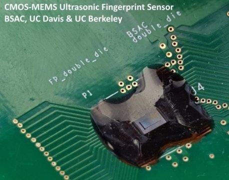
"We developed arrays of PMUTs, along with a custom application-specific integrated circuit (ASIC) and the supporting electronics," Horsley said. "Our work was so successful that we spun off Chirp Microsystems, in 2013, to commercialize it." Shortly before then, in 2011, while exploring other uses for their PMUT technology, they quickly realized that fingerprint sensing was an ideal fit.
"Luckily, we recruited a group of exceptional students to realize our vision, as well as partners within the industry -- our co-authors at InvenSense Inc. and a few other companies -- who funded the work and fabricated our designs," Horsley said.
The basic concepts behind the researchers' technology are akin to those of medical ultrasound imaging. They created a tiny ultrasound imager, designed to observe only a shallow layer of tissue near the finger's surface. "Ultrasound images are collected in the same way that medical ultrasound is conducted," said Horsley. "Transducers on the chip's surface emit a pulse of ultrasound, and these same transducers receive echoes returning from the ridges and valleys of your fingerprint's surface."
The basis for the ultrasound sensor is an array of MEMS ultrasound devices with highly uniform characteristics, and therefore very similar frequency response characteristics.
To fabricate their imager, the group employed existing microelectromechanical systems (MEMS) technology, which smartphones rely on for such functions as microphones and directional orientation. They used a modified version of the manufacturing process used to make the MEMS accelerometer and gyroscope found in the iPhone and many other consumer electronics devices.
fingerprint sensor MEMS CMOS Ultrasonic 相关文章:
- Fingerprint Cards提高对2015年第二季度及全年的营收预期(05-18)
- 指纹识别:没有智能手机,我一样活得很好(03-15)
- OrthAlign全新KneeAlign? 2系统采用ADI运动传感器 提高全膝关节置换术精度 (08-27)
- Sensordynamics被Maxim收购 (06-19)
- Manz亚智科技推出新一代显示器和触摸屏生产解决方案(07-25)
- 传感器让植物“开口”,渴了冷了全知道(11-15)