ADP1046:隔离DC-DC副边应用控制器应用详解(独家)
ing, control, and protection of the power supply output. This information is available through the I2C interface. All voltage sense points can be calibrated digitally to minimize errors due to external components. This calibration can be performed in the production environment, and the settings can be stored in the EEPROM of the ADP1046 (see the Power Supply Calibration and Trim section for more information).
For voltage monitoring, the VS1, VS2, and VS3 voltage value registers (Register 0x15, Register 0x16, and Register 0x17, respectively) are updated every 10 ms. The ADP1046 stores every ADC sample for 10 ms and then outputs the average value at the end of the 10 ms period. Therefore, if these registers are read at least every 10 ms, a true average value is read.
The ADP1046 uses two separate sensing points: VS1 and VS3±, depending on the condition of the OrFET. When the OrFET is turned off, the control loop is regulated via VS1; when the OrFET is turned on, the control loop is regulated via the differential sensing on VS3±. This sensing mechanism effectively performs a local and remote voltage sense.
The control loop of the ADP1046 features a patented multipath architecture. The output voltage is converted simultaneously by two ADCs: a high accuracy ADC and a high speed ADC. The complete signal is reconstructed and processed in the digital filter to provide a high performance, cost competitive solution.
模数转换器
Two kinds of Σ-Δ ADCs are used in the feedback loop of the ADP1046: a low frequency (LF) ADC that runs at 1.56 MHz and a high frequency (HF) ADC that runs at 25 MHz.
Σ-Δ ADCs have a resolution of one bit and operate differently from traditional flash ADCs. The equivalent resolution obtain-able depends on how long the output bit stream of the Σ-Δ is sampled.
Σ-Δ ADCs also differ from Nyquist rate ADCs in that the quan-tization noise is not uniform across the frequency spectrum. At lower frequencies, the noise is lower, and at higher frequencies, the noise is higher (see Figure 4).
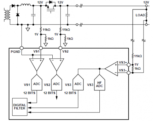
Figure 4
The low frequency ADC runs at approximately 1.56 MHz. For a specified bandwidth, the equivalent resolution can be calculated as follows:
ln(1.56 MHz/BW)/ln2 = N bits
For example, at a bandwidth of 95 Hz, the equivalent resolution/noise is
ln(1.5 MHz/95)/ln2 = 14 bits
At a bandwidth of 1.5 kHz, the equivalent resolution/noise is
ln(1.56 MHz/1.5 kHz)/ln2 = 10 bits
The high frequency ADC has a clock of 25 MHz. It is comb filtered and outputs at the switching frequency (fSW) into the digital filter. The equivalent resolution at some sample frequencies is listed in Table 5.
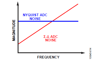
Figure 5
The HF ADC has a range of ±30 mV. Using a base switching frequency (fSW) of 100 kHz (8-bit HF ADC resolution), when fSW increases to 200 kHz (7-bit HF ADC resolution), the quantization noise is 0.9375 mV (1 LSB). Increasing fSW to 400 kHz increases the quantization noise to 3.75 mV (1 LSB = 2 × 30 mV/26 = 0.9375 mV).
推荐阅读:
ADP1046:隔离DC-DC副边应用控制器快速入门指南
摘要: ADP1046 是一款灵活的数字副边控制器,设计用于AC-DC和隔离DC-DC副边应用。ADP1046与ADP1043A引脚兼容,具有一些性能改进和新特性,包括 电压前馈、改进环路响应,以及可编程死区控制,以实现最高效率。内置的EEPROM允许对集成的环路滤波器、PWM信号时序、浪涌电流和软启动时序进行广 泛的编程。通过内置校验和及可编程保护电路,可靠性得以提高。
- ADP1046:隔离DC-DC副边应用控制器快速入门指南(08-09)
- ADP1046:隔离DC-DC副边应用控制器开发必读(独家)(10-11)
- 如何使低功耗放大器在便携式产品中提高性能(10-03)
- D类放大器原理详解及应用设计指南(三)(03-16)
- ADMC331在全数字化逆变电源中的应用(06-20)
- 雷达天线电源故障检测电路的设计(01-27)