ADP1046:隔离DC-DC副边应用控制器应用详解(独家)
ADP1046是一款灵活的数字副边控制器,设计用于AC-DC和隔离DC-DC副边应用。ADP1046与ADP1043A引脚兼容,具有一些性能改进和新特性,包括电压前馈、改进环路响应,以及可编程死区控制,以实现最高效率。
ADP1046还为实现最低元件数量、最大灵活性和最少设计时间进行了优化。具体特性包括本地和远程电压检测、原边和副边电流检测、数字脉宽调制(PWM)产生、均流和冗余OrFET控制。控制环路数字滤波器和补偿功能已集成至该器件,可通过I2C 接口编程。可编程保护功能包括过流保护(OCP)、过压保护(OVP)、欠压闭锁(UVLO)和过温保护(OTP)。
内置的EEPROM允许对集成的环路滤波器、PWM信号时序、浪涌电流和软启动时序进行广泛的编程。通过内置校验和及可编程保护电路,可靠性得以提高。
全面的GUI简化了环路滤波器特性的设计和安全特性的编程。工业标准I2C总线可用于访问许多监控和系统测试功能。
ADP1046提供32引脚LFCSP封装,采用3.3 V单电源供电。
控制理论
电流检测
The ADP1046 has two current sense inputs: CS1 and CS2±. These inputs sense, protect, and control the primary input current, secondary output current, and the share bus information. They can be calibrated to reduce errors due to external components.
CS1操作(CS1)
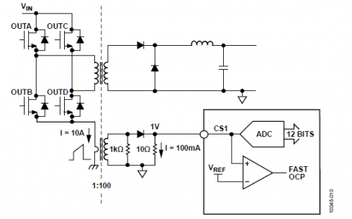
CS1 is typically used for the monitoring and protection of the primary side current, which is commonly sensed using a current transformer (CT). The input signal at the CS1 pin is fed into an ADC for current monitoring. The range of the ADC is 0 V to 1.4 V. The input signal is also fed into a comparator for pulse-by-pulse OCP protection. The typical configuration for the CS1 current sense is shown in Figure 1.

Figure 1
The CS1 ADC is used to measure the average value of the primary current; the reading is averaged every 2.62 ms in an asynchronous fashion to make fault decisions. The ADP1046 also writes the 12-bit CS1 reading every 10 ms to Register 0x13.
The fast OCP comparator is used to limit the instantaneous primary current within each switching cycle and has a nominal threshold of 1.2 V.Various thresholds and limits can be set for CS1, as described in the Current Sense and Current Limit Registers section.
CS2 操作(CS2+, CS2−)
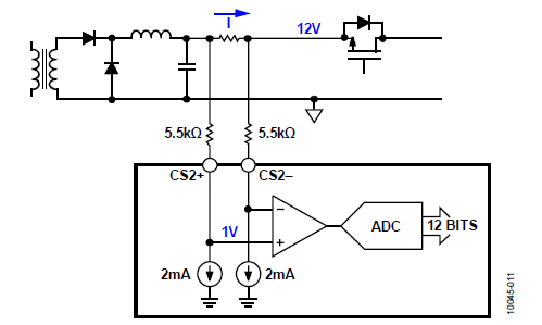
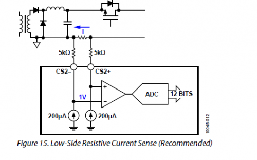
CS2+ and CS2− are differential inputs used for the monitoring and protection of the secondary side current. The full-scale range of the CS2 ADC is programmable to 60 mV or 120 mV. The differential inputs are fed into an ADC through a pair of external resistors that provide the necessary level shifting. The device pins, CS2+ and CS2−, are internally regulated to approxi-mately 1 V by internal current sources.
When using low-side current sensing, the current sources are 200 μA; therefore, the required resistor value is 1 V/200 μA = 5 kΩ. When using high-side current sensing, the current sources are 2 mA; therefore, the resistor value required is (VOUT − 1 V)/2 mA. In the case of VOUT = 12 V, the required resistor value is 5.5 kΩ.
Typical configurations are shown in Figure 2 and Figure 3. Various thresholds and limits can be set for CS2±, such as OCP. These thresholds and limits are described in the Current Sense and Current Limit Registers section.

Figure 2

Figure 3
When not in use, the CS2+ and CS2− inputs should both be connected directly to PGND, and CS2± should be set to high-side current sense mode (Register 0x27[2] = 1).
The CS2 ADC is used to measure the CS2 current; the reading is averaged every 2.62 ms in an asynchronous fashion. This averaged reading is used to make fault decisions, such as the CS2 OCP fault. The ADP1046 also writes the 12-bit CS2 reading every 10 ms to Register 0x18.
电压检测
Multiple voltage sense inputs on the ADP1046 are used for the monitor
- ADP1046:隔离DC-DC副边应用控制器快速入门指南(08-09)
- ADP1046:隔离DC-DC副边应用控制器开发必读(独家)(10-11)
- 如何使低功耗放大器在便携式产品中提高性能(10-03)
- D类放大器原理详解及应用设计指南(三)(03-16)
- ADMC331在全数字化逆变电源中的应用(06-20)
- 雷达天线电源故障检测电路的设计(01-27)
