IGLOO的FPGA构成的马达控制方案
本文介绍了IGLOO系列主要特性和优势,IGLOO系列架构框图以及采用AGL125的马达控制子板主要特性,步进马达控制逻辑方框图,BLDC马达控制逻辑方框图以及马达控制子板电路图和材料清单。
Actel公司的IGLOO系列FPGA是采用Flash Freeze技术的低功耗闪存FPGA,它基于130nm闪存工艺,具有最低功耗,单片解决方案和小占位面积的封装,可重新编程以及丰富的其它特性,核电压1.2 V -1.5 V,支持低功耗和单电压系统工作,Flash Freeze模式的功耗为5uW,系统门从15K到100万,多达144kb的双端口SRAM和多达300个用户I/O,可满足消费品,工业,医疗,汽车电子,计算,通信和军用航天领域的便携产品对低功耗的需要。
IGLOO系列主要特性和优势:
Low Power
? 1.2 V to 1.5 V Core Voltage Support for Low Power
? Supports Single-Voltage System Operation
? 5 μW Power Consumption in Flash*Freeze Mode
? Low Power Active FPGA Operation
? Flash*Freeze Technology Enables Ultra-Low Power Consumption while Maintaining FPGA Content
? Easy Entry to / Exit from Ultra-Low Power Flash*Freeze Mode
High Capacity
? 15 k to 1 Million System Gates
? Up to 144 kbits of True Dual-Port SRAM
? Up to 300 User I/Os
Reprogrammable Flash Technology
? 130-nm, 7-Layer Metal, Flash-Based CMOS Process
? Live-at-Power-Up (LAPU) Level 0 Support
? Single-Chip Solution
? Retains Programmed Design When Powered Off
? 250 MHz (1.5 V systems) and 160 MHz (1.2 V systems) System Performance
In-System Programming (ISP) and Security
? Secure ISP Using On-Chip 128-Bit Advanced Encryption Standard (AES) Decryption (except ARM?-enabled IGLOO? devices) via JTAG (IEEE 1532–compliant)?
? FlashLock? to Secure FPGA Contents
High-Performance Routing Hierarchy
? Segmented, Hierarchical Routing and Clock Structure
Advanced I/O
? 700 Mbps DDR, LVDS-Capable I/Os (AGL250 and above)
? 1.2 V, 1.5 V, 1.8 V, 2.5 V, and 3.3 V Mixed-Voltage Operation
? Bank-Selectable I/O Voltages—up to 4 Banks per Chip
? Single-Ended I/O Standards: LVTTL, LVCMOS 3.3 V / 2.5 V / 1.8 V / 1.5 V / 1.2 V, 3.3 V PCI / 3.3 V PCI-X,and LVCMOS 2.5 V / 5.0 V Input?
? Differential I/O Standards: LVPECL, LVDS, B-LVDS, and MLVDS (AGL250 and above)
? Wide Range Power Supply Voltage Support per JESD8-B, Allowing I/Os to Operate from 2.7 V to 3.6 V
? Wide Range Power Supply Voltage Support per JESD8-12, Allowing I/Os to Operate from 1.14 V to 1.575 V
? I/O Registers on Input, Output, and Enable Paths
? Hot-Swappable and Cold-Sparing I/Os?
? Programmable Output Slew Rate? and Drive Strength
? Weak Pull-Up/-Down
? IEEE 1149.1 (JTAG) Boundary Scan Test
? Pin-Compatible Packages across the IGLOO Family
Clock Conditioning Circuit (CCC) and PLL?
? Six CCC Blocks, One with an Integrated PLL
? Configurable Phase Shift, Multiply/Divide, Delay Capabilities, and External Feedback
? Wide Input Frequency Range (1.5 MHz up to 250 MHz)
Embedded Memory
? 1 kbit of FlashROM User Nonvolatile Memory
? SRAMs and FIFOs with Variable-Aspect-Ratio 4,608-Bit? RAM Blocks (×1, ×2, ×4, ×9, and ×18 organizations)
? True Dual-Port SRAM (except ×18)?
ARM Processor Support in IGLOO FPGAs
? M1 IGLOO Devices—Cortex?-M1 Soft Processor Available with or without Debug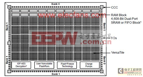
图1。IGLOO系列架构框图(AGL015, AGL030, AGL060和AGL125)
马达控制子板
The Motor Control daughtercard provides a design reference and evaluation kit for motor control using Actel’s ultra-low power IGLOO? FPGAs. This daughtercard, co-developed with Actel and Ishnatek, is available exclusively from Avnet Memec. The board is designed to work with Actel’s IGLOO Icicle? Kit (ordered separately) and attaches to the Icicle kit’s accessory board edge connector.
马达控制子板主要特性:
? Supports
Stepper Motor (4-Wire Configuration)
Full Step / Half Step Mode
Micro Step Mode (Trapezoidal Option)
8 / 16 Microsteps
Brushless DC (BLDC) Motor (Three Phase BLDC Motor)
Sensored Drive
? Using Hall Effect Sensors provided on Motors
? Direction Control – Clockwise or Counterclockwise Rotation
? Basic Functions
Start
Stop
Step ( Full or Half Stepping in case of Stepper Motor)
RPM+/RPM- (Increase/Decrease RPM)
Digital Control Features
? Support Two PWM Modes
PWM on high side of Mosfet Bridge
PWM on low side of Mosfet Bridge (Available but not supported)
? Hardware/Software Control
Access to all above features through keys/switches on board
Equivalent controls are provided also through software
Software Interface using on-board USB-to-RS232 bridge on Icicle
? High Output Current up to 2 A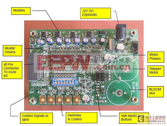
图2。马达控制子板外形图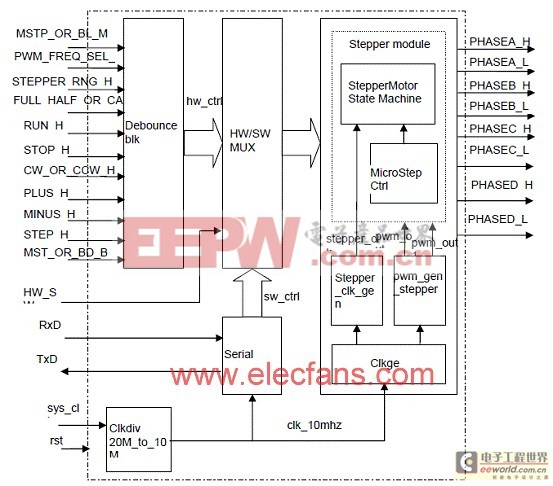
图3。步进马达控制逻辑方框图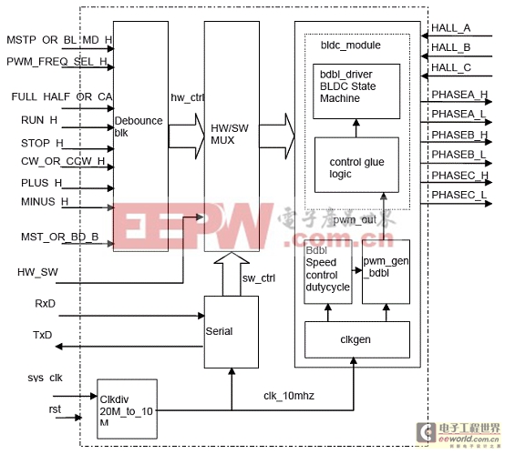
图4。BLDC马达控制逻辑方框图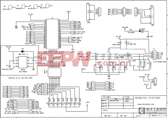
图5。马达控制子板电路图(1)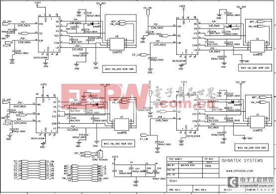
图6。马达控制子板电路图(2)
图7。马达控制子板电路图(3)
马达控制子板材料清单(BOM):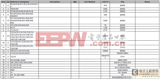
- 在采用FPGA设计DSP系统中仿真的重要性 (06-21)
- 基于 DSP Builder的FIR滤波器的设计与实现(06-21)
- 基于FPGA的快速并行FFT及其在空间太阳望远镜图像锁定系统中的应用(06-21)
- 3DES算法的FPGA高速实现(06-21)
- 用FPGA实现FFT算法(06-21)
- FPGA的DSP性能揭秘(06-16)