深入理解ARM体系架构(S3C6410)---S3C6410系统时钟
在电源控制逻辑中,S3C6410 有多种电源管理方案,以保持电力系统的最佳消耗。In the power control logic, S3C6410X has various power managementschemes to keep optimal power consumption for a given task.
1、在S3C6410中,通用时钟门控模式用来控制内部外设时钟的开/关。可以通过用于外设所要求的特定应用提供时钟,使用通用时钟门控模式来优化S3C6410的电源消耗。例如:如果定时器没有要求,则可以中断时钟定时器,以降低功耗。General Clock Gating mode is used to control the ON/OFF of clocksfor internal peripherals in S3C6410X. You can optimize the power consumption ofS3C6410X using this General Clock Gating mode by supplying clocks for peripheralsthat are required for a certain application. For example, if a timer is notrequired, then you can disconnect the clock to the timer to reduce power.
2、闲置模式仅中断ARMCLK到CPU 内核,它提供时钟给所有外设。通过使用闲置模式,电力消耗通过CPU
内核而减少。
3、停止模式通过禁用PLL冻结所有时钟到CPU 以及外设。在S3C6410 中,电力消耗仅因为漏电流。
4、睡眠模式断开内部电源。因此,除了唤醒逻辑单元消耗的电量,CPU和内部逻辑消耗电量将为零。为了使用睡眠模式,两个独立的电源是必需的。其中一个电源为唤醒逻辑提供电力,另一个提供其他内部逻辑,包括CPU。SLEEP mode disconnects the internal power.Therefore, the power consumption due to CPU and the internal logic except thewakeup logic will be zero. In order to use the SLEEP mode two independent powersources are required. One of the two power sources supplies the power for thewake-up logic. The other one supplies the other internal logic including CPU,and must be controlled in order to be turned ON/OFF. In SLEEP mode, the secondpower supply source for the CPU and internal logic will be turned off.
3.1 系统控制器的特性
The System Controller includes the following features:
• Three PLLs: ARM PLL, main PLL, extra PLL (for the modules those usespecial frequency)
• Five power-saving mode: NORMAL, IDLE, STOP, DEEP-STOP, and SLEEP
• Six controllable power domain: domain-G, domain-V, domain-I,domain-P, domain-F, domain-S
• Control operating clocks of internal sub-blocks
• Control bus priority
3.2 功能描述
这部分主要介绍S3C6410 系统控制器的功能。包含时钟的体系结构,复位设计和电源管理模式。
1、硬件结构
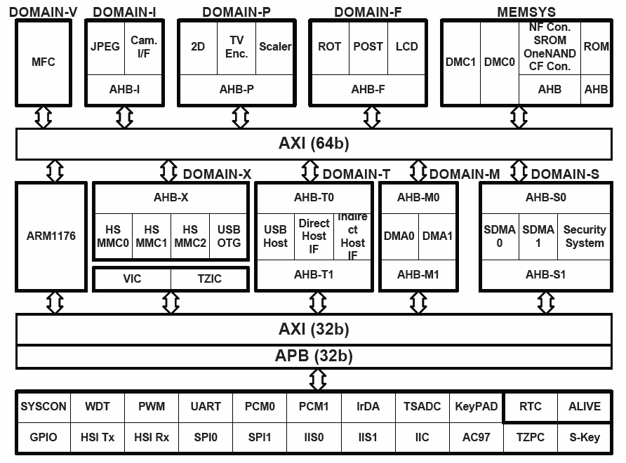
S3C6410是由ARM1176核、一些多媒体协处理器(co-processors)、多种外设IPs组成。ARM1176核是通过64位AXI总线与存储控制器相连的,这样做是为了满足带宽的需要。多媒体协处理(MFC多格式编码器、JPEG、camera接口、TV译码器、3D加速器等)器被分为五个电源域,这五个电源域可被单独控制以降低功耗。S3C6410X consists of ARM1176 processor, several media and graphicco-processors and various peripheral IPs. ARM1176 processor is connected toseveral memory controllers through 64-bit AXI-bus. This is done to meetbandwidth requirements. Media and graphic coprocessors, which include MFC(Multi-Format Codec), JPEG, Camera interface, TV encoder, 3D accelerator and etc,are divided into six power domains. The six power domain can be controlledindependently to reduce unwanted power consumption when the IPs is not requiredfor an application program.
2、时钟结构
时钟源在外部晶振和外部时钟二者之间进行选择。时钟发生器由三个
ARM体系架构S3C6410系统时 相关文章:
- Windows CE 进程、线程和内存管理(11-09)
- RedHatLinux新手入门教程(5)(11-12)
- uClinux介绍(11-09)
- openwebmailV1.60安装教学(11-12)
- Linux嵌入式系统开发平台选型探讨(11-09)
- Windows CE 进程、线程和内存管理(二)(11-09)