深入理解ARM体系架构(S3C6410)---S3C6410系统时钟
PLL组成,最高可产生1.6GHz的信号。
3.时钟源的选择
The OM[4:0] pins determines theoperating mode of S3C6410X when the external reset signal is asserted. Asdescribed in the table, the OM[0] selects the external clock source, i.e., ifthe OM[0] is 0, the XXTIpll (external crystal) is selected.
Otherwise, XEXTCLK is selected.
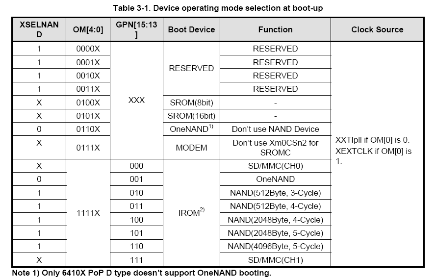
The operating mode is mainlyclassified into six categories according to the boot device. The boot devicecan be among SROM, NOR, OneNAND, MODEM and Internal ROM. When NAND Flash deviceis used, XSELNAND pin must be 1, even if it is used as boot device or storagedevice. When OneNAND Flash device is used, XSELNAND must be 0, even if it isused as boot device or storage device. When NAND/OneNAND device is not used,
XSELNAND can be 0 or 1.
4、锁相环
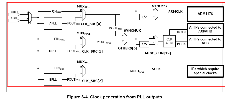
Clock selection betweenPLLs and input reference clock
Figure 3-4illustrates the clock generation logic. S3C6410X has three PLLs which are APLLfor ARM operating clock, MPLL for main operating clock, and EPLL for specialpurpose. The operating clocks are divided into three groups. The first thing isARM clock, which is generated from APLL. MPLL generates the main system clocks,which are used for operating AXI, AHB, and APB bus operation. The last group isgenerated from EPLL. Mainly, the generated clocks are used for peripheral IPs,i.e., UART, IIS, IIC, and etc. The lowest three bits of CLK_SRC registercontrol the source clocks of three groups. When the bit has 0, then the inputclock is bypassed to the group. Otherwise, the PLL output will be applied tothe group.
1)ARM和AXI/AHB/APB时钟
ARM1176最大支持667MHZ,在不改变PLL的情况下,可以通过divarm来控制该频率。
S3C6410由AXI、AHB、APB总线组成。IPs可以连接相应总线来满足I/O带宽和操作性能。连接在AXI/AHB的总线上的设备,最高可以达到133MHz的速度。当连接在APB总线上时,最高可以达到66MHz的速度。总线速度很高程度上依赖于AHB和APB总线之间的同步数据传输。
ARM and AXI/AHB/APB bus clock generation
ARM1176 processor of S3C6410X runs up to maximum 667MHz. Theoperating frequency can be controlled by the internal clock divider, divARM,without changing PLL frequency. The divider ratio varies from 1 to 16. ARM processordecreases the operating speed to reduce power dissipation.S3C6410X consists ofAXI bus, AHB bus, and APB bus to optimize the performance requirements.Internal IPs are connected to appropriate bus systems to meet their I/Obandwidth and operating performance. When they are attached to AXI bus or AHBbus, the operating speed can be up to maximum 133MHz. While they are attachedto APB bus, the maximum operating speed can be up to 66MHz. Moreover, the busspeed between AHB and APB has high dependency to synchronize data transmission.Figure 3-5 illustrates the part of bus clock generation to meet therequirements of bus system clocks.
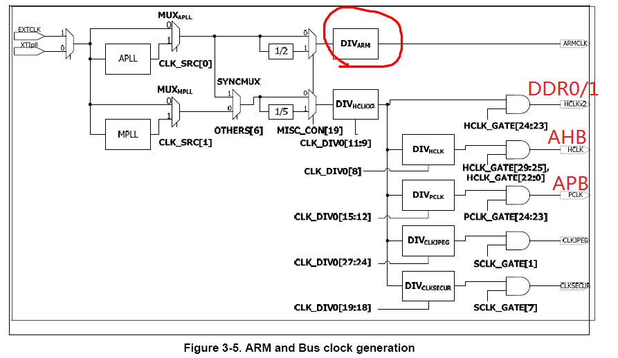
HCLKx2用于两个DDR控制器,DDR0、DDR1,最高可达到266MHZ,每个DDR控制器可以单独控制,以用来降低功耗。所有的AHB总线上的时钟是由divhclk分频得来的,同样,也可以单独控制来降低功耗。HCLK_GATE寄存器来配置HCLKx2和HCLK。
APB总线与AHB总线类似,但是注意:在AHB和APB总线之间的频率比必须隔着一个偶数值,例如:如果divhclk是1,那么divpclk必须是1、3…..,否则,则不能传输数据。
Low-speed interconnection IPs transfer data through APB bus system.APB clocks of them are running at up to 66MHz as described in the above sectionand generated from divPCLK clock divider. They are also masked using PCLK_GATEregister. As described, the frequency ratio between AHB clock and APB clockmust be an even integer value. For example, if divHCLK has 1 of CLK_div0[8],then divPCLK must be 1, 3, ... of CLK_div0[15:1
ARM体系架构S3C6410系统时 相关文章:
- Windows CE 进程、线程和内存管理(11-09)
- RedHatLinux新手入门教程(5)(11-12)
- uClinux介绍(11-09)
- openwebmailV1.60安装教学(11-12)
- Linux嵌入式系统开发平台选型探讨(11-09)
- Windows CE 进程、线程和内存管理(二)(11-09)