隔离式电源电信应用-Isolated Power Suppl
时间:04-13
来源:互联网
点击:
- Feedback via auxiliary transformer windings
- Feedback via optocouplers
- Feedback via extra magnetic parts, which allow communication between the primary and the secondary circuits
To obtain optocoupler feedback, an op amp on the secondary side (such as the MAX4122) continuously compares the output voltage with that generated by a voltage reference (such as the MAX6002). The op-amp output then drives the optocoupler diode, producing a feedback signal from the optocoupler proportional to the error difference between output and reference voltages. That is, a current transfer between the diode and the transistor (isolated from each other) produces a current output on the primary side. Flowing through a resistor, this current produces the signal voltage read by the primary-side controller (Figure 3).
By offering a wide choice of optocouplers already approved for this function by the safety agency, today's market aids safety qualification of the power supply. To further simplify procurement, all components in this circuit are standard parts.
For feedback using extra magnetic parts (which allow communication between the primary and the secondary circuits), the principle is the same as for an optocoupler. The secondary circuit is somewhat complex in this case, because the magnetic parts must be driven by a signal of a certain frequency rather than a DC current. The resulting extra expense of the feedback element (magnetic part) makes this solution less interesting, except for particular applications such as space equipment, in which the higher reliability of a magnetic part is appreciated.
Closing a feedback loop means designing a high-gain wide-bandwidth circuit that allows a fast response to line and load variations. Limits imposed by stability considerations, however, usually compel a compromise on the response time. Two parameters must be defined: crossover frequency (fC) and phase margin.
Overall gain in the feedback path (op amp, optocoupler, and primary controller) has a certain bandwidth, and the corner is that frequency at which the gain equals 1 (0dB). The op amp's inverting configuration introduces a 180° phase shift in the signal (negative feedback), and additional phase lag is introduced by the compensation network. Thus, the signal can exhibit a phase shift of 180° plus 180° or more, producing positive feedback that results in oscillation of the output voltage.
According to Nyquist, a system is stable if the added phase shift at fC is less than 180°. Therefore, a key parameter in power-supply design is phase margin at fC, defined as follows: How many degrees must be added to the feedback phase shift to obtain 180°?
Practical experience with various topologies has shown that a phase margin of 45° allows good load regulation with acceptable overshoot and undershoot, without permitting fast transients to trigger oscillation. Another good compromise is to limit the corner frequency: fC fSWITCHING/(2x3.14xD), where D is the maximum duty cycle.
Every power-supply feedback loop must be designed. Bode plots, offering a simple picture of gain and phase for the different elements, give an overall result when you add the pictures together (Figure 11). Bode says the gain slope for a single pole above its corner frequency is -20dB/decade and its phase shift is 90°. Thus, a double-pole LC network has a gain slope of -40dB/ decade a bove its corner frequency and a phase shift of 180°.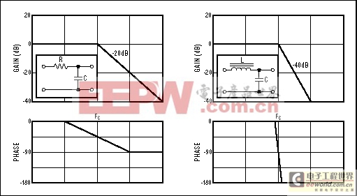
Figure 11. These Bode plots depict a single-pole RC network and a double-pole LC network.
As an example, consider the compensation of a power supply operating at 70kHz with a duty cycle of 50%, described by the power-supply characteristic of Figure 12. The maximum corner frequency is fSWITCHING/(2x3.14xD) = 22kHz. Beyond this corner frequency, the output capacitor, the inductor, and the load resistor produce a -40dB/decade attenuation and a 180° phase shift. The op amp's bandwidth is more than 10MHz, but its associated RC components introduce a pole and zero, to compensate phase lag introduced by the LC pole and to provide at least 45° of phase margin at fC.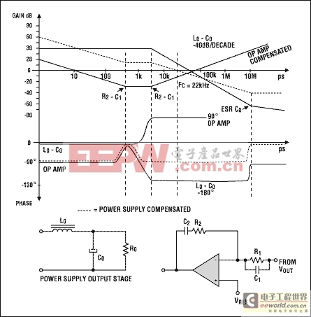
Figure 12. Simplified Bode plots depict a power-supply output and its compensation network.
To ensure good output-voltage regulation at DC, a pole in the error amplifier reduces the gain by -20dB/decade. A zero caused by R2-C2 modifies the gain slope to 0dB/decade, and R2-C1 causes a gain increase to +20dB/decade. As a result, phase introduced by the compensated op amp starts at -90° (due to the first pole), goes to 0° (due to R2-C2), and rises to +90° (due to R2-C1). Summing the output-LC and compensated-op-amp characteristics gives the overall result (dotted line), which indicates a power supply compensated with fC = 22kHz and a phase margin of 90°.
________________________
1Per the American UL Standard (also adopted by the European EN60950 Standard), clearance is the minimum-allowed distance specified for separation of uninsulated conductive surfaces of opposite polarity. Creepage is a corresponding distance between two such surfaces, measured along any connecting surfaces (rather than the line-of-sight through-air distance specified for clearance).
2Per the American UL Standard (also adopted by the European EN60950 Standard), pollution degree 2 environments can have nonconductive contaminants or temporary conductivity caused by condensation. Pollution degree 3 environments can have conductive contaminants.
模拟电源 电源管理 模拟器件 模拟电子 模拟 模拟电路 模拟芯片 德州仪器 放大器 ADI 相关文章:
- 采用数字电源还是模拟电源?(01-17)
- 模拟电源管理与数字电源管理(02-05)
- 数字电源正在超越模拟电源(03-19)
- 数字电源PK模拟电源(04-03)
- TI工程师现身说法:采用数字电源还是模拟电源?(10-10)
- 开关电源与模拟电源的分别(05-08)