隔离式电源电信应用-Isolated Power Suppl
时间:04-13
来源:互联网
点击:
To ensure compliance with all international standards, the designer of an isolated power supply for telecom applications needs to take certain facts into account: The input voltage is never 110V or 220V from the mains, but the lower voltage of a lead-acid battery (-12V, -24V, or -48V) that is charged by means of the mains through rectification (Figure 1). (Batteries back up the telecom system in case of failure in the mains supply.) To combat corrosion due to ion flow, the input voltage is always negative, with the positive terminal connected to ground.

Figure 1. In this block diagram of the backup architecture used in telecom systems, a battery block is kept charged by the mains rectifier. In the event of a mains failure, it supplies the system to prevent transmission interruptions.
ISDN and other systems powered by a remote source often operate with a higher input voltage: up to 120VDC. (Losses due to line resistance are proportional to the square of supply current, so the lower supply current associated with higher input voltage allows a longer transmission line.) By powering the telecom phone through the cable as well as the local mains, such systems eliminate the need for a backup battery at the cable's user end. When required, the cable therefore carries both transmission signals and supply current (Figure 2).
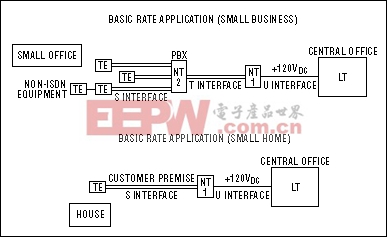
Figure 2. In an ISDN system for small-office or home applications, the phone lines normally carry forward transmissions. During emergencies, they carry power from the central office to the remote unit's network termination (NT) and terminal equipment (TE).
The selection of power-conversion topology depends on the level of output power required: forward or flyback for low power, push-pull for medium power, and half or full bridge for high power. The simplest configuration (flyback) stores energy in the transformer during the ON period of the primary PWM (when the power MOSFET is ON), and it releases it to the load during the OFF period (Figure 3). Because the secondary diode (D1) is forward-biased at that time, energy stored in the transformer goes to the load and charges the output capacitor. Energy stored in the output capacitor is delivered to the load during the next ON period. For this configuration, the primary-controller IC can have a fixed-frequency PWM configuration such as the MAX668 or a variable-frequency PFM configuration such as the MAX1771. A controller like the MAX5003 can be powered directly from the high input voltage.

Figure 3. A flyback converter stores energy during every cycle: in the transformer when the power MOSFET is ON and forward to the load when the power MOSFET is OFF.
In the forward topology (Figure 4), energy is forwarded to the secondary when the primary's power MOSFET turns ON. Energy is not stored in the transformer as in a flyback circuit, so the forward configuration allows a smaller transformer and more power output. An output inductor on the secondary side stores energy and also reduces ripple current in the output capacitor. During an ON period, the load receives energy directly from the transformer trough diode D1 and L1; however, during an OFF period, inductor L1 forces diode D2 to conduct. Thus, L1 and C1 together maintain a continuous delivery of energy to the load.

Figure 4. Because forward converters forward energy to the secondary side during every cycle, they don't require a large isolation transformer for storing energy.
The push-pull configuration (Figure 5) can be simplified as a double-forward converter in which the primary's two power MOSFETs alternate on and off. Energy-conversion principles for the push-pull and forward types are exactly the same during each half cycle, but push-pull circuits reset the transformer during each primary-to-secondary energy transfer (rather than during an OFF period). This action allows more output power for a given transformer geometry.
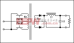
Figure 5. Push-pull converter.
Full-bridge configurations are generally used for power outputs over 1kW (Figure 6). They allow use of the transformer in two quadrants of the BH magnetization characteristic, rather than one as in the forward and flyback circuits (Figure 7). Also, the input-voltage swing seen by the transformer primary equals 2VIN rather than 1VIN. As the power MOSFET pair Q1/Q4 turns on together, then Q2/Q3, the transformer primary winding sees +VIN during the first cycle and -VIN during the second. Energy transfers to the load during each cycle of the secondary (as for the forward topology), but the better transformer optimization allows higher output power.
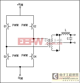
Figure 6. Full-bridge converter.
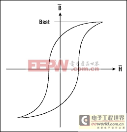
Figure 7. B-H magnetization shape of a magnetic material.
Yet other topologies are available. Resonant or quasi-resonant converters, for example (based on a resonant circuit inserted in the energy-conversion chain), reduce switching-power loss in the active element by avoiding square-wave signals of current and voltage. Whatever the topology, however, points common to all must be taken into consideration:
Figure 1. In this block diagram of the backup architecture used in telecom systems, a battery block is kept charged by the mains rectifier. In the event of a mains failure, it supplies the system to prevent transmission interruptions.
ISDN and other systems powered by a remote source often operate with a higher input voltage: up to 120VDC. (Losses due to line resistance are proportional to the square of supply current, so the lower supply current associated with higher input voltage allows a longer transmission line.) By powering the telecom phone through the cable as well as the local mains, such systems eliminate the need for a backup battery at the cable's user end. When required, the cable therefore carries both transmission signals and supply current (Figure 2).
Figure 2. In an ISDN system for small-office or home applications, the phone lines normally carry forward transmissions. During emergencies, they carry power from the central office to the remote unit's network termination (NT) and terminal equipment (TE).
The selection of power-conversion topology depends on the level of output power required: forward or flyback for low power, push-pull for medium power, and half or full bridge for high power. The simplest configuration (flyback) stores energy in the transformer during the ON period of the primary PWM (when the power MOSFET is ON), and it releases it to the load during the OFF period (Figure 3). Because the secondary diode (D1) is forward-biased at that time, energy stored in the transformer goes to the load and charges the output capacitor. Energy stored in the output capacitor is delivered to the load during the next ON period. For this configuration, the primary-controller IC can have a fixed-frequency PWM configuration such as the MAX668 or a variable-frequency PFM configuration such as the MAX1771. A controller like the MAX5003 can be powered directly from the high input voltage.
Figure 3. A flyback converter stores energy during every cycle: in the transformer when the power MOSFET is ON and forward to the load when the power MOSFET is OFF.
In the forward topology (Figure 4), energy is forwarded to the secondary when the primary's power MOSFET turns ON. Energy is not stored in the transformer as in a flyback circuit, so the forward configuration allows a smaller transformer and more power output. An output inductor on the secondary side stores energy and also reduces ripple current in the output capacitor. During an ON period, the load receives energy directly from the transformer trough diode D1 and L1; however, during an OFF period, inductor L1 forces diode D2 to conduct. Thus, L1 and C1 together maintain a continuous delivery of energy to the load.
Figure 4. Because forward converters forward energy to the secondary side during every cycle, they don't require a large isolation transformer for storing energy.
The push-pull configuration (Figure 5) can be simplified as a double-forward converter in which the primary's two power MOSFETs alternate on and off. Energy-conversion principles for the push-pull and forward types are exactly the same during each half cycle, but push-pull circuits reset the transformer during each primary-to-secondary energy transfer (rather than during an OFF period). This action allows more output power for a given transformer geometry.
Figure 5. Push-pull converter.
Full-bridge configurations are generally used for power outputs over 1kW (Figure 6). They allow use of the transformer in two quadrants of the BH magnetization characteristic, rather than one as in the forward and flyback circuits (Figure 7). Also, the input-voltage swing seen by the transformer primary equals 2VIN rather than 1VIN. As the power MOSFET pair Q1/Q4 turns on together, then Q2/Q3, the transformer primary winding sees +VIN during the first cycle and -VIN during the second. Energy transfers to the load during each cycle of the secondary (as for the forward topology), but the better transformer optimization allows higher output power.
Figure 6. Full-bridge converter.
Figure 7. B-H magnetization shape of a magnetic material.
Yet other topologies are available. Resonant or quasi-resonant converters, for example (based on a resonant circuit inserted in the energy-conversion chain), reduce switching-power loss in the active element by avoiding square-wave signals of current and voltage. Whatever the topology, however, points common to all must be taken into consideration:
模拟电源 电源管理 模拟器件 模拟电子 模拟 模拟电路 模拟芯片 德州仪器 放大器 ADI 相关文章:
- 采用数字电源还是模拟电源?(01-17)
- 模拟电源管理与数字电源管理(02-05)
- 数字电源正在超越模拟电源(03-19)
- 数字电源PK模拟电源(04-03)
- TI工程师现身说法:采用数字电源还是模拟电源?(10-10)
- 开关电源与模拟电源的分别(05-08)