MAX1470电路调整以及与天线的匹配
时间:04-19
来源:互联网
点击:
How to Tune and Antenna Match the MAX1470 Circuit
The MAX1470evkit is tuned and tested at the factory to obtain the highest sensitivity possible. It may however be necessary to "adapt" this circuit to a different frequency or to tune the customer's own pcb. The following application note describes how to accomplish this task.
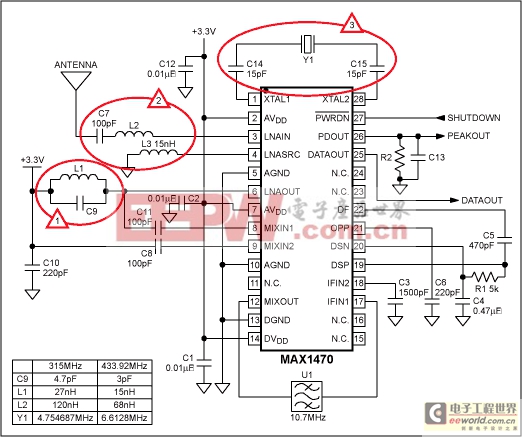
Figure 1 shows a typical MAX1470-based circuit. There are 3 areas of possible tuning to improve RF performance:
- LNA tank tuning
- Input matching and degeneration inductor
- Crystal pulling

Figure 1. MAX1470 typical circuit.
Tuning the LNA Tank
The LC tank filter connected to LNAOUT consists of L1 and C9. L1 = 27nH and C9 = 4.7pF values are selected to resonate at the RF input frequency of 315MHz. The resonant frequency is given by:LTOTAL and CTOTAL include L1 and C9, in addition to parasitic inductance and capacitance of the PC board traces, package pins, mixer input impedance, LNA output impedance, etc. These parasitics cannot be ignored and can have a dramatic effect on the tank filter center frequency.
In order to get the most sensitivity out of the circuit, the tank needs to be tuned as closely to 315MHz (or the frequency of interest) as possible. Therefore, the user will have to determine to what frequency the board is actually tuned and then make component adjustments. This is best accomplished by removing the crystal and directly injecting the crystal frequency with the help of a signal generator. Amplitude should be about 50mVp-p. Set the RF amplitude to -70dBm. Monitor the RSSI output (pin 19). Since the RSSI output will be greatest at the tuned frequency, it's only a question of finding where the max is. Set the RF frequency increment to 640KHz, and the signal generator to 10KHz. As these two are moved in conjunction, the RSSI amplitude will change and will go through a maximum. For example, let's assume that the tank is tuned to 345MHz instead of 315MHz. Assuming a trace inductance of 5nH (based on the length of the trace on the PCB), LTOTAL = 32nH, implying a CTOTAL of 7.98pF at 315MHz. Since, the tank is actually resonating at 345MHz, the actual total capacitance must then be 6.65pF. Therefore, in order to oscillate at 315MHz, CTOTAL must be increased by 1.3pF and C9 must thus be changed to 6pF.
Input Matching and Degeneration Inductor
The off-chip inductive degeneration is achieved by connecting inductor L3 = 15nH from LNASRC (pin 4) to AGND. This inductor (in addition to the 7nH of trace inductance on the evkit PCB) sets the real part of the input impedance at LNAIN to 50 Ωs. Capacitor C7 is a DC blocking capacitor and should be a large capacitor (100pF or more). Since, the LNA input can be modeled as a 50Ω resistor (as long as L3 = 15nH and the trace inductance is 7nH) in series with a 2.5pF capacitor, the S11 of the LNA is given by:S11 = 50-j200 (315MHz) and S11 = 50-j145 (433.92MHz)
L2 is thus needed to match the LNA to 50 Ωs (or other antenna impedance). Therefore, in order to match the MAX1470 to a 50Ω antenna, one only needs to cancel out the -j term. This can easily be accomplished with L2, which would need to be (at 315MHz).
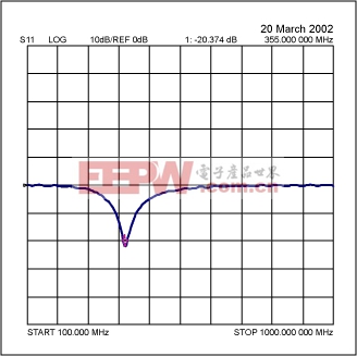
L2 = 200/2 × 3.14 × 315e6 = 100nHA look at the S11 with the help of the network analyzer will allow this to be tuned even better. Set the test port power of the network analyzer to -30dBm so as not to saturate the input stage. Figure 2 shows the S11 of a not so perfectly matched board. The S11 is tuned to 355MHz instead of 315MHz.

Figure 2. S11 plot of RFIN. Match is at 355MHz.
Replacing the 100nH inductor with a 355/315 × 100 = 120nH, allows for a better match as seen in Figure 3.
模拟电路 模拟芯片 德州仪器 放大器 ADI 模拟电子 相关文章:
- 12位串行A/D转换器MAX187的应用(10-06)
- AGC中频放大器设计(下)(10-07)
- 低功耗、3V工作电压、精度0.05% 的A/D变换器(10-09)
- PIC16C5X单片机睡眠状态的键唤醒方法(11-16)
- 用简化方法对高可用性系统中的电源进行数字化管理(10-02)
- 利用GM6801实现智能快速充电器设计(11-20)
