Building a DC-DC power supply
时间:10-25
来源:互联网
点击:
Component placement
When laying out the PCB for this example, you should first place the DC-DC converter IC (e.g., the MAX1742), the inductor, and the input and output capacitors. Then, move those components so the input capacitor is close to the MAX1742's input pins; the inductor is close to the IC's LX pin; and the output capacitor is close to the inductor and the IC's ground pins. Optimizing all of these component positions may require compromises, depending on the IC pin locations. In Maxim's DC-DC converter ICs, pin locations are carefully selected for circuit performance and ease of PCB layout.The most critical node in most cases is the common ground between the input and output capacitors and the ground pin of the IC. These three grounds must be very close, usually within 10mm of each other (Figures 2aand2b). During the charge cycle (Figure 2a), current flows from the input capacitor through the high-side switch, inductor, output capacitor, across the ground plane, and back into the input capacitor. During the discharge cycle (Figure 2b) current continues to flow through the inductor, output capacitor, across the ground plane, back through the IC's ground pin, through the low-side switch, and back into the inductor.
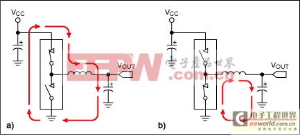
Figure 2. These diagrams illustrate current paths during step-down DC-DC converter's charge (a) and discharge (b) cycles.
Because this circulating current can interfere with other circuits, its path length must be kept short (Short paths also contribute to stable operation and efficiency). Too long a path length in the ground portion (during either cycle) can compromise the circuit's reference for other circuit elements. That condition can also lead to poor regulation, excessive output ripple, and even instability. Placing the input capacitor ground, output capacitor ground, and IC ground adjacent to each other minimizes those unwanted effects.
Another important consideration for the ground connections of current-carrying components is to use multiple parallel PCB vias if the ground plane is on another PCB layer. This is especially important for input and output filter capacitors. A single via often adds resistance and inductance in series with the capacitor, reducing its effectiveness.
Power ground
After placing components according to the criteria above, the common ground is connected either with wide traces or with a polygon of solid copper. Use as much copper as possible to create a low-impedance path between the elements.Local ground
The typical application circuit for many DC-DC converter ICs indicates multiple symbols for ground—this is an excellent hint on how to accomplish a successful circuit layout. One of the different symbols often indicates a local ground plane and is typically titled SGND or AGND. Elements that connect to the local ground plane can include reference-bypass capacitors, resistor-dividers, and resistors that set operating points (such as resistor RTOFFin the example), but should not include high-current grounds such as those from switch MOSFETs.The local ground plane is a solid copper polygon best tied to the power ground plane atone pointonly, typically the pin titled PGND. Local ground planes prevent switching currents from polluting the low-noise local ground plane. Those switching currents often exceed 10A.
Ground plane
Because many systems rely on a separate ground plane for all components on the PCB, it is often tempting to use the ground plane of the DC-DC converter section for that purpose.That temptation should be avoided.The switching currents mentioned above can cause ground glitches across the board, produce excessive EMI, cause invalid logic states, raise the noise level, and cause instability. The proper interface between DC-DC converter circuitry and the ground plane is a single via (or a small grouping of multiple vias), leading from the poured copper power ground to the buried ground plane.Signal routing
After completing the initial ground layout, make the required connections for the first four critical components and then place and route the remaining components. A useful approach is to take all noncritical signals to the backside of the PCB with small vias while reserving the top side of the board for the routing of critical high-current traces.When routing nonpower traces on circuit boards, consider the DC and AC components of the signal. Remember that every trace is a resistor and an inductor, and may also capacitively couple to other traces. Each signal's use in the circuit determines the optimal trace width and length. High-speed and high-current signals demand short, wide traces. Longer, thinner traces are acceptable for less critical signals such as low-speed logic. Route high-speed switching nodes away from sensitive analog areas like the compensation network and feedback node. Also keep the compensation and feedback networks as small as possible to prevent noise pickup. When provided, refer to the layout and grounding guidelines on the PCB layout of the EV kit for more help.
Verification
After the converter is completed, and prototype boards assembled, the overall design should be verified for performance to the original criteria. If the design was implemented diligently with regard to the issues discussed, chances for initial success are good. But even conscientious designs may still require "tweaking." When making changes, verify with calculations or models to be sure that some other important characteristic is not being compromised. For example, you may determine that output ripple is acceptable with smaller output filter capacitance, but such a change might also impact stability.Efficiency
Efficiency is often a key DC-DC converter performance parameter, particularly for devices operating from a battery, and especially so for power supplies in laptop computers and small handheld equipment. Laptop power-supply efficiency directly affects battery life, but it also impacts power dissipation; it should be coordinated with the heat-removal limitations. Note that a DC-DC converter supplying 50W at 85% efficiency still dissipates 8.8W of heat inside the case.In laptops, efficiency is important over a wide range of operating conditions. Examples include low battery, full battery, and battery charging under both standby and operating states. In other applications, the efficiency-critical points depend on how the device is used. Light-load efficiency and quiescent operating current can be most important in small handheld device like a personal glucose meter, while full-load efficiency and heat generation are most critical in network hardware.
Load regulation
A converter's ability to stay within the specified output-voltage tolerance, regardless of load, is called load regulation. It applies at DC, but it also includes fast transients such as those encountered with high-speed CPUs. You should verify that the output voltage stays within specification when loaded with currents ranging from zero to the maximum. Ensure that the output voltage does not undershoot its minimum value when the load changes quickly from minimum to maximum. Ensure that it does not exceed its maximum value when the load current drops from maximum to minimum. Note that the line- and load-regulation specs quoted in most data-sheet electrical characteristics tables are measured at DC, while transient performance is usually shown in the typical operating curves. For more information, see application notes 752, "Creating a fast load transient," and 3453, "Testing a power supply for line and load transients."Line regulation
A power supply's ability to maintain output-voltage regulation with a varying input voltage is called line regulation. Again, it should be examined both at DC and with a fast AC transient. A transient is encountered when a laptop computer switches from its AC adapter supply to its internal battery and back. In some systems, the voltage change can be as large as 10V. Verify that the output voltage stays within specification when the input voltage changes from minimum to maximum. Make sure that step changes in the input voltage do not cause peaks or valleys in the output voltage that exceed the output-voltage specifications.Temperature sensitivity
It may be convenient to evaluate a system on a lab bench and judge it ready for the application, but one more critical condition needs examination: performance over the worst-case operating-temperature range. Performance to the electrical criteria above should be measured at the highest and lowest temperatures that the system will encounter during operation. Watch for parameters that change drastically and those that approach upper or lower limits over temperature.The best way to evaluate a system over temperature is to use an environmental chamber. The chamber lets you conduct computer-controlled experiments over a broad range of temperatures and with an accuracy of 1°C or better. In cases where a chamber is not possible, you can still get an idea of overtemperature performance with less sophisticated equipment. Common heat guns and even hairdryers are useful in heating a circuit while under test. To cool a circuit well below ambient temperature, spray it with a compressed inert gas cold spray (offered in many technical catalogs). When cooling components, avoid condensation. If condensation does occur, understand that a circuit fluctuation might be due to moisture on the circuit board and not circuit sensitivity to temperature.
Conclusion
DC-DC power-supply design is neither rocket science nor common knowledge. The list of characteristics that need to be addressed in a successful design may seem daunting, but a methodical approach can result in a working circuit with minimal iteration. By applying the principles in this article, you can eliminate most of the typical first-design missteps.Maxim offers EV kits for most of its DC-DC converters. Maxim's free EE-Sim simulation tool can also be used for more reliable power supply designs, and is available for a growing number of power supply devices.
- 新型灌封式6A至12A DC-DC μModule稳压器系列(11-19)
- DC-DC开关变换器中混沌现象的研究综述(11-27)
- 数码相机电源电路设计及DC/DC变换器选择(01-22)
- 产生双极性输出的无变压器 DC/DC 变换器(01-23)
- 改进型全桥移相ZVS-PWMDC/DC变换器(01-23)
- 为DC/DC转换器选择正确的电感器与电容器(01-02)