Building a DC-DC power supply
时间:10-25
来源:互联网
点击:
This article discusses important considerations when designing a DC-DC power supply. Topics include choosing the right DC-DC converter for the application; MOSFET gate capacitance; high switching frequencies and component size; equations and calculations; selecting peripheral components; component placement and trade-offs; grounding; load and line regulation; temperature sensitivity.
Also see:
There are few comprehensive sources of DC-DC design information. Engineering textbooks discuss control theory, loop compensation, and other highly detailed analytical methods. Data sheets for DC-DC converters give specific formulas and some layout information. Less information is available to guide the overall design of integrated-circuit-based DC-DC converters from start to finish.
This article fills in information gaps for a first DC-DC power supply design. It is the result of the author's failures and successes with scores of power-supply circuits.
Note that a boost DC-DC converter output will rise with input voltage when the input exceeds what has been set for the output voltage. Similarly, a buck converter cannot provide the desired output when the input voltage is less than that output. It is said to be "in dropout" when that happens.
Many DC-DC load requirements can be met by DC-DC converter ICs that include integral power switches. Most such ICs include MOSFETs, but some employ bipolar transistors. The load current capability of newer internal MOSFET DC-DC ICs can handle up to 25A (e.g., theMAX8655andMAX8686). An internal-switch device, if available, is usually preferred, both for overall simplicity and (often) for lower total cost.
High-power or high-voltage applications that exceed the abilities of internal-MOSFET devices will need external MOSFET switches. DC-DC converters designed for driving external power switches are usually called "controllers." These ICs include drivers for quickly charging and discharging an external MOSFETs' gate capacitance. The ability to quickly charge and discharge a MOSFET gate is critical in achieving high-efficiency conversion. The switch wants to spend as little time as possible in transition between its on and off states because that is when power loss is greatest. Most DC-DC controllers specify a maximum gate capacitance that they can drive. (See the section, MOSFET gate capacitance below.)
In addition to topology, voltage, and current considerations, there are likely to be other application characteristics that direct the choice of DC-DC IC. For example, in most automotive applications a DC-DC converter should be able to tolerate cold-crank and load-dump conditions as well as a -40°C to +125°C temperature range. Maxim's on-line parametric search tool helps choose among converter features and specifications.
In circuits where the source voltage does change during switching, the more useful dynamic parameter is reverse transfer capacitance (CRSS). CRSSis used in calculating switching loss in a high-side n-Channel MOSFET of a buck converter in accordance with the following equation:
The next most common control scheme is pulse-frequency modulation (PFM), where the converter supplies switching pulses only when required by the load. PFM converters excel in applications that require low quiescent current and high efficiency at very small loads. Some converters ICs employ both schemes to combine good idle-mode efficiency with low noise.
The switching frequencies of IC DC-DC converters and controllers range from 65kHz to over 4MHz. In general, it is probably best to avoid devices that operate below 100kHz, as such frequencies are typical of old devices with poor efficiency. Higher switching frequency allows smaller external components along with lower peak currents and I2R losses, but core losses, gate-charge currents, and switching losses increase. (See the section on High-switching frequency reduces component size.) If the application demands the smallest possible size, then look for converters with switching frequencies at 1MHz and above. Otherwise, simply choose a device that meets the power criteria and verify that its switching frequency does not interfere with other components in the system.
Higher switching frequency also reduces the size of the output capacitor. In the example above, the capacitance required is 67μF at 500kHz, but only 33μF at 1MHz. The ripple-current specification remains unchanged.
After choosing a particular device type (buck, boost, etc.), make the final selection by consulting DC-DC converter manufacturers' websites. Always check the manufacturer's website for the latest data sheet. While there, look for application notes that apply to the device that you are considering. They serve as a guide and often include circuits that can be used with little or no modification. (See: Power Supply Cookbook, Maxim's power supply application notes, and the power and battery-management products.)From application notes and data sheets you can obtain the equations that govern the design for your device.
As an example, consider the MAX1742, an internal-switch buck converter. The data sheet's Design Procedure section gives necessary information and the order for calculations. We assume a constant 5V input, a 3.3V output with maximum load current of 500mA, and a 500kHz operating frequency.
Use the defined variable names whenever possible. As you enter more equations, define the results of those calculations with more names. Choose the names so you can easily remember what they mean when you check the calculations later.
First, across the top of a new worksheet, enter names for all predetermined values (Figure 1). These names might include VINMIN, VINMAX, VOUT, IOUT, FREQ (frequency), and other terms associated with the converter. In the cells immediately beneath the cells containing those names, define cell names to match the names typed above.
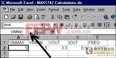
Figure 1. Using cell names in spreadsheets.
To define a cell name: select the cell to be named, go to the Insert menu and select Name, then Define on the submenu. In Excel, a dialog box pops up to suggest (as a default name) the text immediately above the selected cell. To name the cell, click OK on this dialog box. Proceed across the row until all these fields have been named. This naming procedure allows you to refer to VINMAXin your calculations instead of cell A2. Note that the selected cell in Figure 1 is A2, with a value of 5. The cell's name is indicated just above the row labeled A. Next, scan through the design procedure and pick all the required component values (Table 1). Note that original spreadsheet values have been converted to SI units for clarity.
Table 1. Initial component calculations
Also see:
- Application note 2031, "DC-DC Converter Tutorial"
- Power Supply Cookbook
Introduction
A designer's first DC-DC converter circuit generally has one thing in common with first attempts in any other field: it has a slim chance of working satisfactorily when first powered. That may sound like a gloomy assessment, but it nevertheless reflects the realities of switch-mode power-supply design. DC-DC converters are complex systems. Even when simplified by highly integrated ICs, they still require extensive component calculations and thoughtful selection of the controller IC. In addition, they are sensitive to board layout and component parasitics (i.e., the characteristics of a component that are not ideal, such as resistance in a capacitor or capacitance in a MOSFET switch).There are few comprehensive sources of DC-DC design information. Engineering textbooks discuss control theory, loop compensation, and other highly detailed analytical methods. Data sheets for DC-DC converters give specific formulas and some layout information. Less information is available to guide the overall design of integrated-circuit-based DC-DC converters from start to finish.
This article fills in information gaps for a first DC-DC power supply design. It is the result of the author's failures and successes with scores of power-supply circuits.
Device selection
Once the initial specs of a DC-DC design are selected (e.g., input voltage range, output voltage, output current), the first step is to select a converter IC. The desired DC-DC topology will narrow this choice. If the input voltage is greater than the output voltage, choose a buck (i.e., step-down) topology. If the input voltage is less than the output voltage, choose a boost (i.e., step-up) configuration. If the input voltage ranges above and below the output voltage, a buck-boost converter or a SEPIC converter is needed. Lastly, if the output voltage is negative, an inverting topology is used.Note that a boost DC-DC converter output will rise with input voltage when the input exceeds what has been set for the output voltage. Similarly, a buck converter cannot provide the desired output when the input voltage is less than that output. It is said to be "in dropout" when that happens.
Many DC-DC load requirements can be met by DC-DC converter ICs that include integral power switches. Most such ICs include MOSFETs, but some employ bipolar transistors. The load current capability of newer internal MOSFET DC-DC ICs can handle up to 25A (e.g., theMAX8655andMAX8686). An internal-switch device, if available, is usually preferred, both for overall simplicity and (often) for lower total cost.
High-power or high-voltage applications that exceed the abilities of internal-MOSFET devices will need external MOSFET switches. DC-DC converters designed for driving external power switches are usually called "controllers." These ICs include drivers for quickly charging and discharging an external MOSFETs' gate capacitance. The ability to quickly charge and discharge a MOSFET gate is critical in achieving high-efficiency conversion. The switch wants to spend as little time as possible in transition between its on and off states because that is when power loss is greatest. Most DC-DC controllers specify a maximum gate capacitance that they can drive. (See the section, MOSFET gate capacitance below.)
In addition to topology, voltage, and current considerations, there are likely to be other application characteristics that direct the choice of DC-DC IC. For example, in most automotive applications a DC-DC converter should be able to tolerate cold-crank and load-dump conditions as well as a -40°C to +125°C temperature range. Maxim's on-line parametric search tool helps choose among converter features and specifications.
MOSFET gate capacitance
Power MOSFET manufacturers provide various dynamic and switching parameters on their data sheets in addition to DC specs like on-resistance. In most cases, when using external MOSFETs with DC-DC converters, total gate charge (QG) is of primary interest. Choose MOSFETs for which the QGis within the range recommended by the manufacturer of the DC-DC converter. Using the MOSFET's typical QGvalue is fine for most cases. The maximum number is usually overly conservative. The QGspec is used when driving an "open-drain" low-side n-channel or high-side p-channel MOSFET, or in other words, when the MOSFET source does not change voltage during switching.In circuits where the source voltage does change during switching, the more useful dynamic parameter is reverse transfer capacitance (CRSS). CRSSis used in calculating switching loss in a high-side n-Channel MOSFET of a buck converter in accordance with the following equation:
PD(switching) = (CRSS× VIN(MAX)2 × fSW× ILOAD)/IGATEWhere IGATEis the peak gate source and sink current, and fSWis the switching frequency.
PWM and other control schemes
The most popular DC-DC converter control scheme is pulse-width modulation (PWM). PWM converters maintain a constant switching frequency over a broad range of loads. That behavior can be important when switching noise might interfere with other processes in a system. Confining the noise to a known band often mitigates interference.The next most common control scheme is pulse-frequency modulation (PFM), where the converter supplies switching pulses only when required by the load. PFM converters excel in applications that require low quiescent current and high efficiency at very small loads. Some converters ICs employ both schemes to combine good idle-mode efficiency with low noise.
The switching frequencies of IC DC-DC converters and controllers range from 65kHz to over 4MHz. In general, it is probably best to avoid devices that operate below 100kHz, as such frequencies are typical of old devices with poor efficiency. Higher switching frequency allows smaller external components along with lower peak currents and I2R losses, but core losses, gate-charge currents, and switching losses increase. (See the section on High-switching frequency reduces component size.) If the application demands the smallest possible size, then look for converters with switching frequencies at 1MHz and above. Otherwise, simply choose a device that meets the power criteria and verify that its switching frequency does not interfere with other components in the system.
High-switching frequency reduces component size
A continuous trend in DC-DC converters is to higher switching frequencies in order to achieve smaller component sizes. When more switching cycles occur per second, the energy per switching cycle (and the size of the components that store that energy) can be smaller. Inductor values, for instance, can be lower. Inductor behavior is governed by the following equations:VL= L × (di/dt)For example, consider a buck converter operating at 500kHz with a 10μH inductor. Changing the frequency to 1MHz allows exactly one-half the inductance, or 5μH, to be used to achieve the same power transfer. Although the inductance value decreases by one-half, the current requirement remains the same. The second equation shows that we just reduced the inductor's required energy storage by half as well. Since inductance is proportional to the square of the number of turns, reducing inductance by half means the turns count is reduced to 70.7% of the original number. Reducing the turns also proportionally lowers the DC resistance (DCR), so the resulting inductor is smaller and has lower DCR.
WL= (L × i2)/2
Higher switching frequency also reduces the size of the output capacitor. In the example above, the capacitance required is 67μF at 500kHz, but only 33μF at 1MHz. The ripple-current specification remains unchanged.
After choosing a particular device type (buck, boost, etc.), make the final selection by consulting DC-DC converter manufacturers' websites. Always check the manufacturer's website for the latest data sheet. While there, look for application notes that apply to the device that you are considering. They serve as a guide and often include circuits that can be used with little or no modification. (See: Power Supply Cookbook, Maxim's power supply application notes, and the power and battery-management products.)From application notes and data sheets you can obtain the equations that govern the design for your device.
Design equations
DC-DC converter data sheets should contain equations helpful for designing your circuit. Macro models or spreadsheet files for calculating component values may also be available on the product webpage. Be sure to read the IC data sheet carefully to ensure that you select the proper equations for the required performance and operating mode. Once the major design parameters are known and you have the right equations, the best tool for evaluating the equations is a spreadsheet such as Excel? or an engineering-math program such as MathCAD. Maxim's EE-Sim? tool generates an interactive schematic that features a highly efficient simulation engine. If the selected device has an EE-Sim model, use that to calculate the appropriate components for your design.Spreadsheet calculations
Spreadsheets are an effective basic design tool for DC-DC converters. They can even serve as crude circuit simulators, and their "Solve" feature can help optimize component values. When used with DC-DC converter equations, a spreadsheet allows an iterative approach that aids component selection by quickly indicating cause-and-effect relationships.As an example, consider the MAX1742, an internal-switch buck converter. The data sheet's Design Procedure section gives necessary information and the order for calculations. We assume a constant 5V input, a 3.3V output with maximum load current of 500mA, and a 500kHz operating frequency.
Use the defined variable names whenever possible. As you enter more equations, define the results of those calculations with more names. Choose the names so you can easily remember what they mean when you check the calculations later.
First, across the top of a new worksheet, enter names for all predetermined values (Figure 1). These names might include VINMIN, VINMAX, VOUT, IOUT, FREQ (frequency), and other terms associated with the converter. In the cells immediately beneath the cells containing those names, define cell names to match the names typed above.
Figure 1. Using cell names in spreadsheets.
To define a cell name: select the cell to be named, go to the Insert menu and select Name, then Define on the submenu. In Excel, a dialog box pops up to suggest (as a default name) the text immediately above the selected cell. To name the cell, click OK on this dialog box. Proceed across the row until all these fields have been named. This naming procedure allows you to refer to VINMAXin your calculations instead of cell A2. Note that the selected cell in Figure 1 is A2, with a value of 5. The cell's name is indicated just above the row labeled A. Next, scan through the design procedure and pick all the required component values (Table 1). Note that original spreadsheet values have been converted to SI units for clarity.
Table 1. Initial component calculations
- 新型灌封式6A至12A DC-DC μModule稳压器系列(11-19)
- DC-DC开关变换器中混沌现象的研究综述(11-27)
- 数码相机电源电路设计及DC/DC变换器选择(01-22)
- 产生双极性输出的无变压器 DC/DC 变换器(01-23)
- 改进型全桥移相ZVS-PWMDC/DC变换器(01-23)
- 为DC/DC转换器选择正确的电感器与电容器(01-02)