安森美同步整流NCP4330的设计方案
时间:12-20
来源:互联网
点击:
简述:
对于电源而言,既要充分利用电能,又要尽可能地减少不必要的电能损耗。NCP4330内置一个双MOSFET驱动器,用于采用同步整流的交流-直流
或直流-直流多输出后稳压电源中的辅助芯片。直接由次级交流信号供电,
器件将功耗保持最低,同时减少了周围零件数量。
主要特征:
The NCP4330 houses a dual MOSFET driver intended to be used as a companion chip in AC−DC or DC−DC multi−output post regulated power supplies. Being directly fed by the secondary AC signal, the device keeps power dissipation to the lowest while reducing the surrounding part count. Furthermore, the implementation of a N−channel MOSFET gives NCP4330−based applications a significant advantage in terms of efficiency.
Undervoltage Lockout
•Thermal Shutdown for Overtemperature Protection
• WM Operation Synchronized to the Converter Frequency
•High Gate Drive Capability
•Bootstrap for NMOSFET HighSide Drive
•OverLap Management for Soft Switching
•Ideal for Frequencies up to 400 kHz
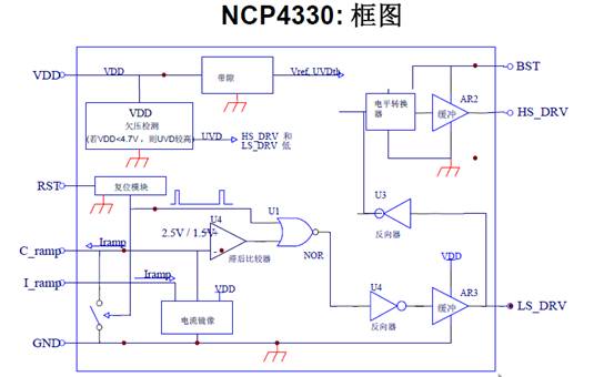
图1 NCP4430 框图
方案特点:
The evaluation board is designed to speed up evaluationof NCP4330 based post regulator SMPS applicationstogether with external traditionally regulated main forwardsupply. NCP4330 Evaluation board is built on one copper layerPCB using mixed (through hole and SMT) mountingtechnology. Large copper areas are used when needed forminimizing parasitic inductances and cooling the surfacemounted power devices (NTMS4700N power FETs,NCP4330 IC and inductor).
参考原理图:
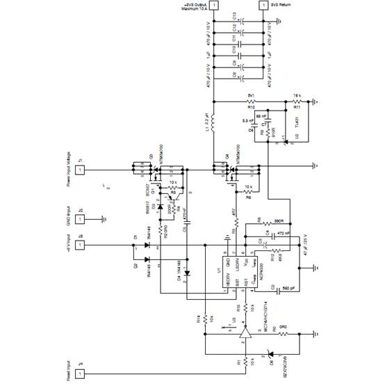
图2 参考原理图1
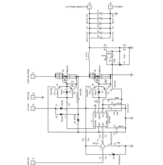
图3 参考原理图2
参考PCB图:
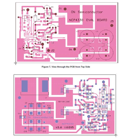
图4 PCB bottom
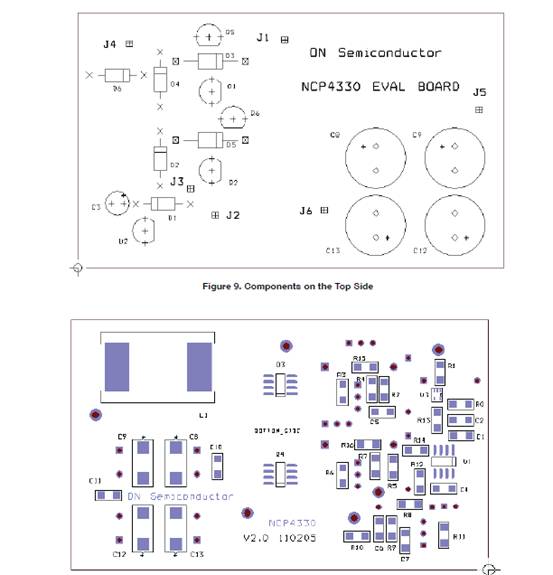
图5 pcb元件图
详情请见:
 NCP4330EVB-D.PDF
(698.41 KB, 下载次数: 6)
下载积分: 积分 -1
(网络)
对于电源而言,既要充分利用电能,又要尽可能地减少不必要的电能损耗。NCP4330内置一个双MOSFET驱动器,用于采用同步整流的交流-直流
或直流-直流多输出后稳压电源中的辅助芯片。直接由次级交流信号供电,
器件将功耗保持最低,同时减少了周围零件数量。
主要特征:
The NCP4330 houses a dual MOSFET driver intended to be used as a companion chip in AC−DC or DC−DC multi−output post regulated power supplies. Being directly fed by the secondary AC signal, the device keeps power dissipation to the lowest while reducing the surrounding part count. Furthermore, the implementation of a N−channel MOSFET gives NCP4330−based applications a significant advantage in terms of efficiency.
Undervoltage Lockout
•Thermal Shutdown for Overtemperature Protection
•
 WM Operation Synchronized to the Converter Frequency
•High Gate Drive Capability
•Bootstrap for NMOSFET HighSide Drive
•OverLap Management for Soft Switching
•Ideal for Frequencies up to 400 kHz

图1 NCP4430 框图
方案特点:
The evaluation board is designed to speed up evaluationof NCP4330 based post regulator SMPS applicationstogether with external traditionally regulated main forwardsupply. NCP4330 Evaluation board is built on one copper layerPCB using mixed (through hole and SMT) mountingtechnology. Large copper areas are used when needed forminimizing parasitic inductances and cooling the surfacemounted power devices (NTMS4700N power FETs,NCP4330 IC and inductor).
参考原理图:

图2 参考原理图1

图3 参考原理图2
参考PCB图:

图4 PCB bottom

图5 pcb元件图
详情请见:
 NCP4330EVB-D.PDF
(698.41 KB, 下载次数: 6)
2012-12-20 13:51:20 上传
下载次数: 6下载积分: 积分 -1
(网络)
- 电源设计小贴士 1:为您的电源选择正确的工作频率(12-25)
- 超低静态电流电源管理IC延长便携应用工作时间(04-14)
- 电源SOC:或许好用的“疯狂”创意(07-24)
- 过压保护及瞬态电压抑制电路设计(04-03)
- 用于低成本高效率离线LED驱动器的初级端调节技术(05-14)
- 隔离式MOSFET驱动器集成电路的功率效率在轻负载时得到改善(07-31)
