EPOT应用:增益调整的运算放大器电路
时间:03-28
来源:本站整理
点击:
Variable gain amplifiers often use a mechanical potentiometer to set the gain. An example is a volume control dial. However, when the analog signal path is digitally controlled, a digital potentiometer might be used to control gain. This article discusses the use of the digital potentiometer to form digitally controlled gain or filter blocks.
Even though the designer needs to adhere to the standard constraints associated with semiconductor devices, (i.e., absolute maximum ratings) there are a couple of characteristics specific to EPOTs that the engineer should keep in mind when using them in op-amp circuits.
One of the first things to remember is that the tolerance of the end-to-end or absolute resistance of digital potentiometers is usually specified for a maximum of ±25% to ±30%. This is mainly due to process variations and a technique for handling this is discussed throughout this article.
Additional things to consider are the characteristics of the EPOT's "wiper". The "wiper" in an EPOT is effectively a string of CMOS switches and will exhibit the typical characteristics. Important specifications for the wiper include its resistance, the variation of its resistance, its maximum current rating and its temperature coefficient. For example, the wiper resistance of the MAX5400 is specified for a typical value of 250 Ω but with a maximum value of 800 Ω. The absolute maximum current rating of the wiper (as well as the rest of resistor in the EPOT) is 1mA. Care should be taken not to exceed this current rating as excessive current can damage the device. Lastly, the temperature coefficient for the wiper is typically about ±300ppm/°C.
One final EPOT consideration is how it will behave near either extreme of the adjustment range. For example, when an EPOT is set to one of its higher or lower settings the ESD structures, such as wiper characteristics, can begin to drastically affect performance. A general rule of thumb is to try and keep the EPOT set to between 10% and 90% of full scale.
In general, the principles described here apply to all of the EPOTs in the Maxim line. The 256 tap EPOT has been chosen for illustration purposes. Internally, an EPOT is viewed as a string of resistors with CMOS switches "tapping" off that string. In linear EPOTs the spacing along the resistor string is even, in logarithmic taper EPOTs, the spacing would be logarithmic. Therefore, an EPOT with a given number (m) of taps has one fewer resistors (m-1). For the purposes of discussion in this article, the variable "n" refers to the absolute setting of the EPOT (i.e., 0 to 31 or 0 to 255 and so on) and "N" refers to the ratio of the setting of the EPOT to its maximum value (i.e., 0 to 1). For example, in a linear taper EPOT with 256 taps a setting of n=89 would give N=0.3490, which is 89/255. "Re" refers to the total end-to-end resistance of the EPOT, thus an EPOT can be thought of as 2 resistors with values N × Re and (1-N) × Re. Furthermore, gain equations are shown in this article as a function of the variable "N" as G(N). The total available range of adjustment is shown as G(0)<=G(N)<=G(1) or as G(1)<=G(N)<=G(0), as applies.
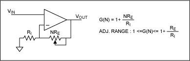
Figure 1a. Circuit 1.
One disadvantage is that because the feedback current flows through the wiper, its resistance (and that resistance's variance with temperature) as well as its maximum current rating (typically about 1mA) may limit the applications for this circuit. Another disadvantage is that the end-to-end resistance, Re, is a part of the gain equation causing the ±25% tolerance of Re to contribute up to a ±25% variance in the gain. Mathematically, the maximum possible contribution of a 25% error in Re to the overall gain is 25%. Of course, as the Re/Ri term in the gain equation becomes smaller and the "1" term begins to dominate the gain, the error as a function of the tolerance of Re becomes smaller.
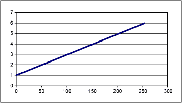
Figure 1b. Gain of circuit 1 with Re=50k and Ri=10k.
Circuit 1 is suited for cost sensitive systems that can live with the somewhat loose tolerance in overall gain. As with many of the circuits seen here, this includes circuits like volume or brightness control where the user is going to iteratively adjust the circuit according to personal preference. Another useful application would be in an automatic gain control circuit where either digital or analog automatic gain control is used to make a gain compensation for a system output. For example, an APD circuit may use either digital or analog automatic gain control to control the biasing of the photodiode with high accuracy. In such a circuit, the automatic gain control technique takes the tolerance of Re (in the EPOT) out of the equation.
Another possible configuration is shown in circuit 2. Here the wiper is connected to the high impedance input of the op-amp using the EPOT as a sort of variable voltage divider. By connecting the wiper to this high-Z input, the only current that flows through the wiper will be the input bias current of the op-amp. This current is typically very small (usually between pA and uA) so that any variance in the several hundred Ω resistance of the wiper will be negligible.
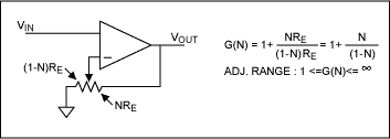
Figure 2a. Circuit 2.
In addition, the Re terms on the top and bottom of the gain equation cancel out leaving just a function of N. This removes the impact of end-to-end resistance from the gain equation altogether.
Unfortunately, this circuit has one big disadvantage. The gain adjustment is non-linear with respect to N. A plot of G(N) for circuit 2 is shown in Figure 2. By deriving the slope of G(N) as G'(N) = 1/(1-N)², it can be seen that the slope is also a function of N and therefore isn't even piecewise linear over a select range of N. In the section on Inverting Configurations, several ways to use this circuit and counteract its inherent non-linearity are discussed.
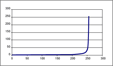
Figure 2b. G(N) for circuit 2.
Circuit 2 is useful in many of the same systems mentioned for circuit 1 (i.e., audio control, brightness control, AGC loops etc.). In addition to the applications seen in circuit 1, the lack of a dependence on Re and the resistance of the wiper makes this an excellent circuit for calibration adjustments. Also notice that in circuit 2, the gain steps are heavily concentrated from 1 to 2, but that much higher gains are still possible. While rare, some calibration applications may call for a period of high gain followed by a period of very finely tuned low gain. An example might be in the measurement of air pressure in a blood pressure cuff. In such a system, when inflation is initiated, the pressure is very low and the measurement is primarily used to detect faults (high gain). Once the cuff is fully inflated the measurements are used to detect minute changes in cuff pressure vs. time. The AGC loop using circuit 2 can be used to optimize ADC dynamic range during blood pressure measurement. The calibration is done at production to compensate for mechanical and sensor deviations.
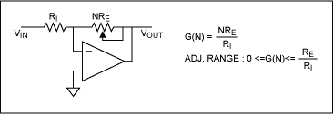
Figure 3a. Circuit 3.
This circuit has the benefit of having a linear gain adjustment as a function of N, as shown in Figure 3b.
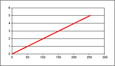
Figure 3b. G(N) for circuit 3 with Re=50k and Ri=10k.
This circuit has the same disadvantages as those seen in circuit 1. It will have a slightly different dependence on the tolerance of Re because the gain equation is slightly different; the gain will vary as much as ±25% as the tolerance on Re varies. This circuit is going to be useful in inverting applications similar to those already mentioned for circuits 1 and 2.
Just like circuit 2, circuit 4 is not susceptible to the disadvantages mentioned for circuits 1 and 3. Because the Re terms on the top and bottom cancel each other out of the gain equation, the gain depends only on N. As a result, errors in the absolute resistance are effectively cancelled out in circuit 4, making it attractive for use with EPOTs that have a wide tolerance for the end-to-end resistance. In addition, an op-amp's input bias current is usually in the range of pA to uA. With so little current flowing through it, the wiper's resistance, drift with temperature and maximum current spec will not be a factor in this circuit.
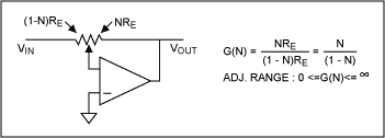
Figure 4a. Circuit 4.
The gain for this circuit is shown in Figure 4b. This circuit has the same drawback as circuit 2, its gain adjustment is going to be non-linear over the entire range of N. This inherently non-linear gain adjustment does not prevent this from being useful. This circuit will fit very well where an inverting amp is needed in the same applications as for circuit 2. For example, this might fit well in applications with user feedback, such as volume control or display brightness control circuits and also in calibration circuits or AGC circuits.
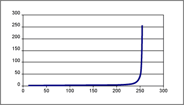
Figure 4b. G(N) for circuit 2 with a 256 tap EPOT.
However, some systems require even gain steps as a function of N. Below, two approaches are given for linearizing the gain of circuit 4.
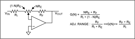
Figure 5a. Circuit 5.
By adding resistors to both the input path and the feedback path, the minimum gain (where N=0) is raised and the maximum gain (where N=1) is lowered effectively compacting the available gain range. For example, in the plot shown the gain can be adjusted from 1 to 3 rather than from the 0 to 255 corresponding circuit 4.
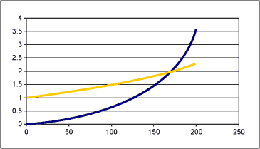
Figure 5b. G(N) for circuit 5 with Ri=50k and Rf=100k (yellow). G(N) for circuit 4 is also shown (blue) for illustration.
This circuit also has the advantage of connecting the wiper to the high impedance op-amp input. Additionally, while the gain is not going to be perfectly linear like circuit 3, any effects the wiper's characteristics have on performance are taken out of the equation by greatly reducing the current through the wiper.
The big drawback to this circuit is that by adding Ri and Rf to the gain equation, the Re terms that were cancelled out in circuit 4 cannot be cancelled out here. One advantage of circuit 4 was that the Re terms in the gain equation cancelled each other out making the large tolerance of the end-to-end resistance irrelevant. For circuit 5 however, the Re terms cannot be cancelled out and deviations in the end-to-end resistance of the EPOT will affect the overall gain. The exact impact of deviations in the end-to-end resistance will depend on the ratio of Rf and Ri to Re. Making Rf and Ri large with respect to Re can minimize this impact, but will hamper the available adjustment range. In the example used for the plot of Figure 5b, a 25% increase in Re makes the minimum gain 0.88 rather than 1 and the maximum gain 3.25 rather than 3. A 25% decrease in Re makes the minimum 1.14 and the maximum 2.75.
The goal for this design is to have the following performance characteristics:
General
Throughout this discussion of digital potentiometers, the term EPOT is used rather than digital pot, EEPOT or E²POT. The term EPOT describes the Maxim series of volatile digital potentiometers, while the other terms describe a variety of non-volatile and volatile devices manufactured on one of several different processes. The specifics of how these different processes affect digital potentiometer performance are outside the scope of this article. While the equations given below can be applied to all digital potentiometer circuits, the special considerations relating to voltage ratings, current ratings are intended specifically for Maxim's EPOT devices.Even though the designer needs to adhere to the standard constraints associated with semiconductor devices, (i.e., absolute maximum ratings) there are a couple of characteristics specific to EPOTs that the engineer should keep in mind when using them in op-amp circuits.
One of the first things to remember is that the tolerance of the end-to-end or absolute resistance of digital potentiometers is usually specified for a maximum of ±25% to ±30%. This is mainly due to process variations and a technique for handling this is discussed throughout this article.
Additional things to consider are the characteristics of the EPOT's "wiper". The "wiper" in an EPOT is effectively a string of CMOS switches and will exhibit the typical characteristics. Important specifications for the wiper include its resistance, the variation of its resistance, its maximum current rating and its temperature coefficient. For example, the wiper resistance of the MAX5400 is specified for a typical value of 250 Ω but with a maximum value of 800 Ω. The absolute maximum current rating of the wiper (as well as the rest of resistor in the EPOT) is 1mA. Care should be taken not to exceed this current rating as excessive current can damage the device. Lastly, the temperature coefficient for the wiper is typically about ±300ppm/°C.
One final EPOT consideration is how it will behave near either extreme of the adjustment range. For example, when an EPOT is set to one of its higher or lower settings the ESD structures, such as wiper characteristics, can begin to drastically affect performance. A general rule of thumb is to try and keep the EPOT set to between 10% and 90% of full scale.
In general, the principles described here apply to all of the EPOTs in the Maxim line. The 256 tap EPOT has been chosen for illustration purposes. Internally, an EPOT is viewed as a string of resistors with CMOS switches "tapping" off that string. In linear EPOTs the spacing along the resistor string is even, in logarithmic taper EPOTs, the spacing would be logarithmic. Therefore, an EPOT with a given number (m) of taps has one fewer resistors (m-1). For the purposes of discussion in this article, the variable "n" refers to the absolute setting of the EPOT (i.e., 0 to 31 or 0 to 255 and so on) and "N" refers to the ratio of the setting of the EPOT to its maximum value (i.e., 0 to 1). For example, in a linear taper EPOT with 256 taps a setting of n=89 would give N=0.3490, which is 89/255. "Re" refers to the total end-to-end resistance of the EPOT, thus an EPOT can be thought of as 2 resistors with values N × Re and (1-N) × Re. Furthermore, gain equations are shown in this article as a function of the variable "N" as G(N). The total available range of adjustment is shown as G(0)<=G(N)<=G(1) or as G(1)<=G(N)<=G(0), as applies.
Non-Inverting Configurations
Circuit 1 is a non-inverting gain configuration using the EPOT as a variable resistor. In this circuit, the wiper is connected to one side of the EPOT effectively shorting out the (1-N) × Re side of the device. As a result, the feedback current flows through wiper and the portion of the EPOT correlating to N × Re. This circuit has a nice linear gain adjustment curve with respect to N, but some of the EPOT's characteristics give this circuit a few disadvantages.Figure 1a. Circuit 1.
One disadvantage is that because the feedback current flows through the wiper, its resistance (and that resistance's variance with temperature) as well as its maximum current rating (typically about 1mA) may limit the applications for this circuit. Another disadvantage is that the end-to-end resistance, Re, is a part of the gain equation causing the ±25% tolerance of Re to contribute up to a ±25% variance in the gain. Mathematically, the maximum possible contribution of a 25% error in Re to the overall gain is 25%. Of course, as the Re/Ri term in the gain equation becomes smaller and the "1" term begins to dominate the gain, the error as a function of the tolerance of Re becomes smaller.
Figure 1b. Gain of circuit 1 with Re=50k and Ri=10k.
Circuit 1 is suited for cost sensitive systems that can live with the somewhat loose tolerance in overall gain. As with many of the circuits seen here, this includes circuits like volume or brightness control where the user is going to iteratively adjust the circuit according to personal preference. Another useful application would be in an automatic gain control circuit where either digital or analog automatic gain control is used to make a gain compensation for a system output. For example, an APD circuit may use either digital or analog automatic gain control to control the biasing of the photodiode with high accuracy. In such a circuit, the automatic gain control technique takes the tolerance of Re (in the EPOT) out of the equation.
Another possible configuration is shown in circuit 2. Here the wiper is connected to the high impedance input of the op-amp using the EPOT as a sort of variable voltage divider. By connecting the wiper to this high-Z input, the only current that flows through the wiper will be the input bias current of the op-amp. This current is typically very small (usually between pA and uA) so that any variance in the several hundred Ω resistance of the wiper will be negligible.
Figure 2a. Circuit 2.
In addition, the Re terms on the top and bottom of the gain equation cancel out leaving just a function of N. This removes the impact of end-to-end resistance from the gain equation altogether.
Unfortunately, this circuit has one big disadvantage. The gain adjustment is non-linear with respect to N. A plot of G(N) for circuit 2 is shown in Figure 2. By deriving the slope of G(N) as G'(N) = 1/(1-N)², it can be seen that the slope is also a function of N and therefore isn't even piecewise linear over a select range of N. In the section on Inverting Configurations, several ways to use this circuit and counteract its inherent non-linearity are discussed.
Figure 2b. G(N) for circuit 2.
Circuit 2 is useful in many of the same systems mentioned for circuit 1 (i.e., audio control, brightness control, AGC loops etc.). In addition to the applications seen in circuit 1, the lack of a dependence on Re and the resistance of the wiper makes this an excellent circuit for calibration adjustments. Also notice that in circuit 2, the gain steps are heavily concentrated from 1 to 2, but that much higher gains are still possible. While rare, some calibration applications may call for a period of high gain followed by a period of very finely tuned low gain. An example might be in the measurement of air pressure in a blood pressure cuff. In such a system, when inflation is initiated, the pressure is very low and the measurement is primarily used to detect faults (high gain). Once the cuff is fully inflated the measurements are used to detect minute changes in cuff pressure vs. time. The AGC loop using circuit 2 can be used to optimize ADC dynamic range during blood pressure measurement. The calibration is done at production to compensate for mechanical and sensor deviations.
Inverting Configurations
The principles used in the non-inverting configurations can also be applied to inverting op-amp circuits. In circuit 3 the gain is simply the apparent resistance in the feedback path over the input resistance.Figure 3a. Circuit 3.
This circuit has the benefit of having a linear gain adjustment as a function of N, as shown in Figure 3b.
Figure 3b. G(N) for circuit 3 with Re=50k and Ri=10k.
This circuit has the same disadvantages as those seen in circuit 1. It will have a slightly different dependence on the tolerance of Re because the gain equation is slightly different; the gain will vary as much as ±25% as the tolerance on Re varies. This circuit is going to be useful in inverting applications similar to those already mentioned for circuits 1 and 2.
Just like circuit 2, circuit 4 is not susceptible to the disadvantages mentioned for circuits 1 and 3. Because the Re terms on the top and bottom cancel each other out of the gain equation, the gain depends only on N. As a result, errors in the absolute resistance are effectively cancelled out in circuit 4, making it attractive for use with EPOTs that have a wide tolerance for the end-to-end resistance. In addition, an op-amp's input bias current is usually in the range of pA to uA. With so little current flowing through it, the wiper's resistance, drift with temperature and maximum current spec will not be a factor in this circuit.
Figure 4a. Circuit 4.
The gain for this circuit is shown in Figure 4b. This circuit has the same drawback as circuit 2, its gain adjustment is going to be non-linear over the entire range of N. This inherently non-linear gain adjustment does not prevent this from being useful. This circuit will fit very well where an inverting amp is needed in the same applications as for circuit 2. For example, this might fit well in applications with user feedback, such as volume control or display brightness control circuits and also in calibration circuits or AGC circuits.
Figure 4b. G(N) for circuit 2 with a 256 tap EPOT.
However, some systems require even gain steps as a function of N. Below, two approaches are given for linearizing the gain of circuit 4.
Linearizing Circuit 4's Gain with Resistors
In circuit 5, resistors have been added to the input path and the feedback path to "flatten out" the plot of the gain. In the plot of G(N) for this circuit, both its gain and the gain for circuit 4 are shown. The last 50 points have been omitted for clarity. This plot shows how the gain curve can be "flattened" at the expense of adjustment range.Figure 5a. Circuit 5.
By adding resistors to both the input path and the feedback path, the minimum gain (where N=0) is raised and the maximum gain (where N=1) is lowered effectively compacting the available gain range. For example, in the plot shown the gain can be adjusted from 1 to 3 rather than from the 0 to 255 corresponding circuit 4.
Figure 5b. G(N) for circuit 5 with Ri=50k and Rf=100k (yellow). G(N) for circuit 4 is also shown (blue) for illustration.
This circuit also has the advantage of connecting the wiper to the high impedance op-amp input. Additionally, while the gain is not going to be perfectly linear like circuit 3, any effects the wiper's characteristics have on performance are taken out of the equation by greatly reducing the current through the wiper.
The big drawback to this circuit is that by adding Ri and Rf to the gain equation, the Re terms that were cancelled out in circuit 4 cannot be cancelled out here. One advantage of circuit 4 was that the Re terms in the gain equation cancelled each other out making the large tolerance of the end-to-end resistance irrelevant. For circuit 5 however, the Re terms cannot be cancelled out and deviations in the end-to-end resistance of the EPOT will affect the overall gain. The exact impact of deviations in the end-to-end resistance will depend on the ratio of Rf and Ri to Re. Making Rf and Ri large with respect to Re can minimize this impact, but will hamper the available adjustment range. In the example used for the plot of Figure 5b, a 25% increase in Re makes the minimum gain 0.88 rather than 1 and the maximum gain 3.25 rather than 3. A 25% decrease in Re makes the minimum 1.14 and the maximum 2.75.
A Design Example using Software Compensation to Linearize Gain
Most systems use a microcontroller to control the setting of the EPOT and therefore, the gain of the circuits here are usually controlled by software. In addition, while this article has used 256 step EPOTs for illustration, many systems only need 20 to 30 steps in the gain. Using software and a 256 step EPOT configured as shown in circuit 4, 20 to 30 steps of linear gain adjustment curve can easily be accomplished by using software compensation. A design example is shown here for a software compensated, inverting, and adjustable gain op-amp circuit.The goal for this design is to have the following performance characteristics:
放大器 相关文章:
- 分析测量放大器的共模抑制能力(09-15)
- 开关模式GaAs功率放大器在WLAN设计中大放异彩(09-30)
- 利用高端电流检测放大器简化模拟电路设计(09-15)
- 运算放大器选择指南 助您获得上佳的噪声性能(09-10)
- 运算放大器组成阶梯波发生器电路图(10-11)
- 电容器与声音的关系(11-04)