LNA IIP3 vs Input RF Power Plot
时间:04-09
整理:3721RD
点击:
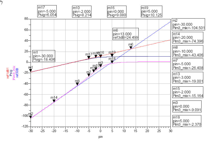
Hi, wonder if anybody come across any plot for LNA IIP3 (sim or measured)? If yes, how does it look like? Have an example, but do not know if it's correct?
The graph that you get is correct. The deep in the characteristic is due to the phases of the third and fifth IMD products. You can minimize this deep placing the bias of the amplifier closer to Class A operating point.
if the input power is less than P1dB above 10dB or more, the ip3 will be same with different input power.
the attached is my simulation result.
This phenomenom is called "Sweet Spot" where the transistor is in the region between weak inversion and saturation, so the third and fifth derivatives of gm is going to 0 so the IIP3 is improved.
How would the third and the fifth IMD products are at the same frequency?
- Different Input/Output matching
- How do you choose input power while doing loadpull?
- Why an input inductor required in all GPS LNA?
- Input and output impedance matching in Distributed amplifier
- In distributed amplifiers, is it total input capacitance of the gain stage or Cgs
- curve fitting for input and output matching