run a simulation
Thanks a lot.
Rgds.
hi there
well you are right you need to create a new folder in the 1D results folder by right clicking and choosing from the popup menu.
however you then need to copy and paste the required results into this folder and rerun the simulation for other results
i hope i answer your question
regards
Thanks Shahid,
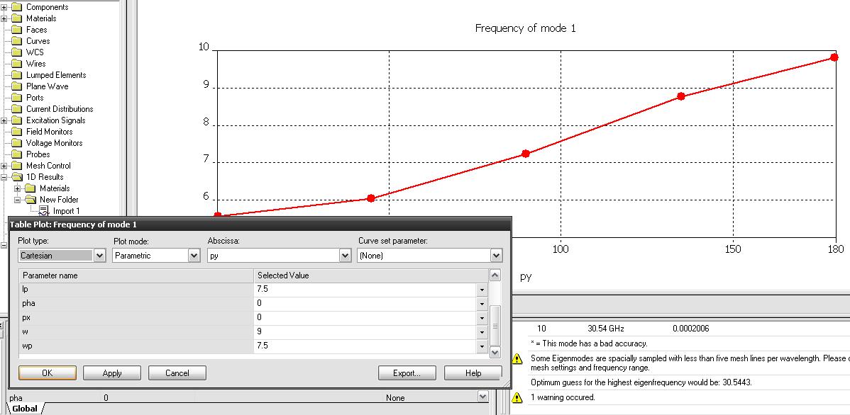
I right clicked on the 1D result folder and chose add new tree folder. I also right clicked on the new folder and chose import result form ASCII file. I think that this must be the data result in Table (freqent mode 1) so I search in my project and see the file freqent mode 1. tab. I know that it must be changed to text file to be imported. Am I right ? So I click Table properties and choose export. But the import results in the new folder is not my result.
Please help me.
hi there
well , as i mentioned in my earlier post , you just need to creat a new folder to store your simulated results.
than right click the results which you want to copy. from the context menu click copy. go to the new folder, right click and select paste , thats it
regards
Hi Shahid,
I've just done as your suggestion and it runs. Thank u so much.
I saw that u have posted many about the dispersion diagram for EBG in CST. So have u found the final result. When i tried in CST, in z+ we must choose the boundary condition: Et=0 or Ht=0 to run in eigenmode. Et=0 for TM mode and the other for TE mode. In the dispersion diagram, the curve at the bottom correspond to TM mode and the upper is TE mode. The gap between them is band gap freq. Am I wrong?. In the Eigenmode there have Frequent mode 1,2... (add watch). Do we have to choose add watch freq mode 2 or higher mode watch to have the dispersion diagram. What your ideas?
Regards.
hi
well after trying many options i have left pursuing how to find the dispersion diagram in cST.
what i have learned , only HFSS is suitable for finding the dispersion diagram for metallo dielectric EBGs
regarding TM and TE modes. well you set the appropriate boundary condition for the TE or TM modes and than you find 2 or 3 higher order TE and TM modes.
for a complete bandgap you must have bandgap for both modes. in the dispersion diagram the two curves which you are mentioning doesnt necessarily means that one is TE mode and other is TM mode
i hope this information is helpful
regards
Dear Shahid78,
Thanks for your reply. I have heard about the S-parameter method for analyzing the bandgap. So can I consruct the finite dimensions EBG (metallic dielectric type) structure and using two waveguide port to have the s21 results. Have u tried this before? If so can u share me some experiences for running it in CST MWS.
Rgds.