PCB layout of Microstrip line BPF question
时间:04-08
整理:3721RD
点击:
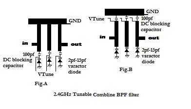
I have a question on the PCB layout of a 2.4GHz tunable combline BPF filter,
It is tunable by changing the voltage of varactor diodes. see the attached picture. There are two possible implementations, Fig.A and Fig.B since the tuning voltage Vtun can not shorted to GND, I need a DC blocking capacitor between the varactor diode and Microstrip lines which is grounded.
the questions is which way is better ? Fig.A or Fig.B
The PCB layout of Fig.A is a little bit messy, Is the series capacitor and diode, may change the length of Microstrip line ?
For the fig.B arrangement what is the DC blocking capacitor should be for varactor diode in 2.4GHz? is the 100pf capacitor good enough to ground the Microstrip line in 2.4GHz frequency?
I prefer A. All your parasitics are in one place at one end of the line. The ground is good. In B, you have parasitics at both ends of the line and the ground is not so good because of the capacitor. You will also need DC blocking capacitors on IN/OUT for B.
For either one, you will need an RF choke in series with the Vtune leads. If you don't the low impedance of the Vtune will short out your RF signal.