transformer amplifier
In Minicircuits datasheet is specified Ratio 4, that means is a 4:1 transformer.
I didn't use Orcad for a while but I think in the library is a 4:1 transformer that you can use.
If you do not have the Spice model for BLF202 try to find in the library an available lower power MOSFET (same frequency range), and use it just to see how the simulation works at low signal level.
but when it says ohm ratio is 4 means the ratio of secondary/primary?
Added after 4 minutes:
and also, is there any way to get .olb and .lib file for orcad from .s2p?so many manufacturers are only giving the .s2p file.
Added after 2 hours 5 minutes:
Hi, now i have the schematic, please take a look!any suggestion?P.S. i'm going to use blf202 for the transistor
and also i keep getting this error saying that "Voltage source and/or inductor loop involving L-L4" Any idea?
Thanks a lot
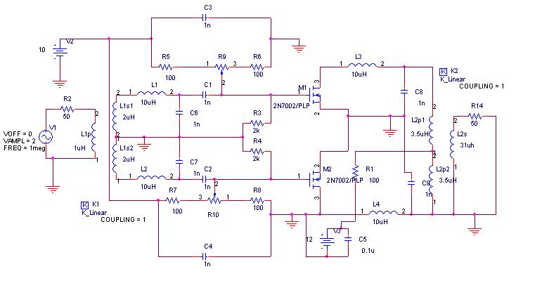
There is a mistake in the schematic. Both pins, 2 and 3 of M2 transistor are grounded.
Thanks, it's a mistake on my schematic because i drew it too quickly, but my board is connected properly(PIN 3 of M2 is not grounded)
Added after 4 minutes:
ok, this is my latest attempt, i use blf 202 and pin 3 of m2 is not grounded. the datasheet of the blf202 says that the VGS is ranging from 2.3-2.4v, so if i set the bias circuits to generate 2.3V each, and the input signal on each transistor is 2Vpp, shouldn't it work?but it doesn't on mine. Thanks
What do you mean with "not working"? Simulation errors as "inductor loop" are something different. They can be avoided by adding real world parameters as a small inductor series resistance. I also wonder about the purpose of using a small signal NF FET rather than a RF power FET in simulation.
No, i'm doing real life experiment, not just simulation. The fet is replaced with BLF202, RF fet from NXP. What i mean not working is that all the signals are fine until it reached the input of each FETs(they were 2Vpp,50MHz, 180 deg out of phase) and i was hoping to get an 4Vpp,50MHz, and 200mA output...but the output is almost 0..let me upload the updated schematic
NOTE: V2 IS 5 INSTEAD OF 10
FETs ARE REPLACED WITH RF FET(BLF202)
thanks!
Added after 1 minutes:
P.S. by output i mean the output of the final transformer
It's hard to operate the amplifier with a that negative gain. As a first step, you should verify a suitable DC bias point. Then trace the RF level through the amplifier and check, if you didn't unintentionally invert one channel and effectively cancel the output signal.
transformer amplifier 相关文章:
- transformer S11 simulation
- Where Can I buy Transformer Core Ferrites for Frequencies ABOVE 200 MHz ?
- Can a transformer be used to convert single ended signal to differential signal?
- asking about quarter wavelength transformer?
- What is the best option to solve too wide quarterwave transformer problem?
- Transformer matching network design