resistor or inductor?
My question is that if it is a good idea to use this resistor instead of an inductor? My concern is that the RF AC signal at the gate of driver transistor may interfere with the biasing voltage source Vg1.(In the picture, it's using depletion mode MESFET and that's why biasing voltage is negative 1. I am using CMOS so it should be positive)
So what do you think the resistor Rg1 is for in the topology in the picture? If it is for biasing, do you think it is a good idea to use it this way? Thanks

The 10K resistor is a pure biasing circuit. Due to the high resistance compared to the circuit impedance level, it hasn't any effect on impedance matching. Apparently the input matching is achieved by Lg1 exclusively, assuming Cb is only working as DC decoupling (no capacitance value given). The circuit doesn't use resistive (lossy) impedance matching at all, by the way. A small band amplifier rarely does.
Lg2 in contrast is a combined impedance matching/biasing element.
You should to ask for the circuit concept as a whole rather than the usage of a particular part. You can't change a single element without affecting the overall behaviour. And you shouldn't do that without understanding the circuit concept.
Thank you very much. It really makes sense to me.
I thought Cb and Lg1 are all part of input impedance matching network although I know Cb is for blocking DC current.
Here are some other questions regarding the desgin:
1. For biasing voltage to the gate of the driver transistor (class F) and output stage transistor (Class E), shall I just use the threshold voltage(Vt) as the biasing point since the two transistors working in switching mode? In the picture, two biasing voltages are different. I am a little confused.
2. Is there a small signal model for transistors working in switching mode (triode and cutoff)? I ask this just because I need to calculate the optimum output impedance.
3. When calculating the interstage impedance between driver and output stages, do I need to consider Cgd of the driver transistor?
Thank you very much!
This article could help:
http://www.cc.ncu.edu.tw/~ncu7020/Fi.../hjj/paper.pdf
Thanks for the paper. I have read that paper before. But I still have the problems listed above I can't answer.
Thanks.
Cannot exist a small signal model for a transistor working in saturation, as Class E and F.
These classes purposely avoids the linear region (or small signal), operating the device only as a switch.
Here you can find some examples which can give an idea how to find the output impedance:
http://www.rfcafe.com/references/art...-Lecture-4.ppt
1-Vbias voltages are different because FET sizes are different.400um vs. 4mm
2-Small dignal models don't represent switching operation mode, they are used only in small signal operating mode.
3-You should of course take Cgd into account while matching.
1.Another question, since both transistors don't have small signal model because they switching mode transistor, how can I calculate interstage impedance between driver stage and output stage? I am trying match the interstage impedance up to 50 ohms.
2.Without the small signal model for impedance matching, the only thing I know I need to consider for the interstage impedance matching is the Vgs and Vgd of the transistor in output stage. How about the transistor in driver stage? Cds or anything from the driver transistor I need take into consideration?
3.Also the two LC parallel tanks are tunned at fundamental and the 3rd harmonic. Since they are tuned, there impedance should be zero right? So I don't need to take the two tanks into consideration on interstage impedance matching right?
Thanks.
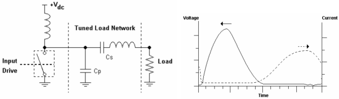
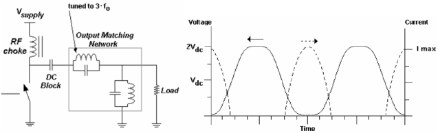
Have to tune the matching networks to get the voltage and currents for each working class (class F for driver, and class E for final) as in the images below.
Well, I know what is in the picture is what I need to achieve. I think not only tuning matching network, but all the components in the circuit.
What I am trying to calculate is the the parameter value of L and C between the drive and output stage. The approach I try to use is to look in to the output of the driver stage until input of the output stage. So I can use conjugate matching to get the value of L and C. Any idea?
- Resistors in N-Way Wilkinson Power Combiner
- Would smd resistor on ridge waveguide (or rgw waveguide) act as series resistor?
- Question about LNA stability resistor
- The function of the resistor connected to the gate of PM20
- What type of resistors, inductors, and capacitors to use for 2 GHz LNA design?
- Varicap driving without current limiting resistor.