What is wrong with my schematics to measure S11 for FET transistor?
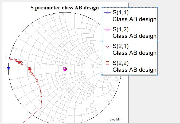
I got this Smithchart from MWO, and according to my supervisor, S11 shouldn't be 0 and S21 S12 shouldn't be 1...but I can't find any problem with my schematics...when I carry out the annotation, the current from port 1 is 40 mA when it's supposed to be 0...no idea why it's that...

Please help!
You have connected the DC bias direct to the gate of the CREE transistor. The DC bias is a voltage source and will appear as a perfect short on the smith chart.
Also you have connected it straight to port 1 without a DC blocking capacitor.
-2V into 50 ohm is -40mA.
Same for port 2.
Try putting an inductor in series with the DC source and a series blocking capacitor on port 1 and port 2.
Better still, if you are serious (are you serious or is this just a windup?) about playing with CREE GaN transistors then contact a CREE rep for assistance. They can offer you basic MWO startup schematics.
Your schematic is also wrong because you have placed a 12 ohm resistor (?) in the drain and also you are only running from 15V. I think you will be advised by CREE to run these devices at at least 20V drain voltage (and probably less than 32V)
What spec amplifier are you hoping to design?
I've designed several broadband amplifiers with these devices.
You forgot the DC blocking capacitors.
And use ideal DC choke coils between DC sources and input/output ports..Voltage sources are short circuit for AC signals..
The other strange thing about this request is that the non linear models for MWO for the CREE GaN parts used to be kept under wraps by CREE. A few years back I had to meet up with CREE reps and sign an NDA to get access to their best models.
Yet this beginner has access to the model?
Are these CREE models freely available nowadays?
Thanks for pointing out the problems, wonder what is the function of DC blocking capacitor?
The 12.25 ohm resistor was calculated from the IV charateristic to get a 10 volt Vds, when Vgs = -2 V, the current is already flat as Vds increases, wonder what is the difference running device at 20 V drain voltage and 10 V drain voltage?
Thanks for the help
The DC blocking cap is there to stop (block) DC from leaking into your test ports.
Sadly I'm not able to give you any detailed advice on designing with this device because I've signed an NDA with CREE. Also I might get told off at my place of work :)
However, I think I can safely point you in the direction of a paper on their website
Try and arrange your MWO circuit to look more like the circuit on page 21 of the pdf presentation below.
Note that CREE tend to only publish very basic MWO schematics so you will have to eventually produce a much more detailed schematic in order to model the PCB layout and component parasitics more effectively.
http://www.cree.com/products/pdf/App..._PA_Design.pdf
Can I ask where you got the CGH40010F_r4a model for this device?
Thank you very much, this model is provided by the project I'm researching on, that's how I got the model.
Hey GHOZU,
After adding a DC blocking capacitor, the drain current start to become extremely big, and does not match the IV characteristics any more, the voltage appearing at the drain is only 0.9 V..wonder why this is happening?
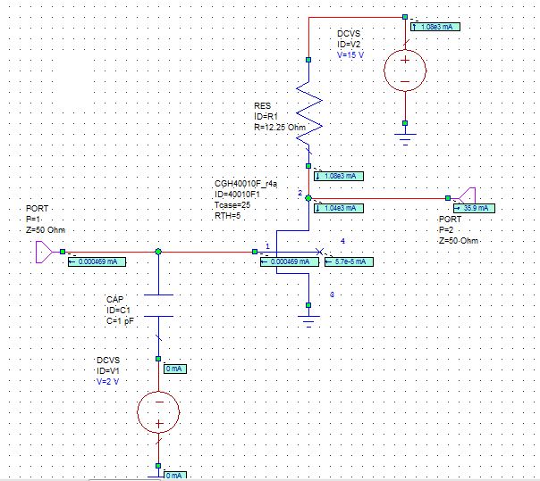
Is it normal for current to flow into port 2?
Thanks
These guys can help you much better than I can
Microsoft Xbox 360 Repairs from Repairs-Direct.com - UK wide collect and return 4 day service.
Why did you place the capacitor in the bias path? The capacitor(s) must be inserted between the circuit and the RF ports.
It must be like this...
It's a waste of time. I gave this person a link in post #6 to a complete MWO schematic for this device complete with test results for simulation and measured results. (from the manufacturer)
The OP is either a troll or too dim to be let loose on this project. In another thread he is designing a piecewise predistorter.
Not bad for someone who can't work out why a capacitor blocks a DC bias?
measure schematics wrong 相关文章:
- How do I know if a spectrum analyzer is enough to measure an specficic DAC?
- Using ADS2019, How to set and measure tempature values for LNA?
- H field measurements with waveguide twist
- How can I measure the Side-Band Amplitude?
- Keysight PNA Harmonics measurements
- frequency shift between simulation and measurements