Drawing Meander inductor in MWO
I am new user of MWO layout. I have designed in schematic meander inductor but not getting the same shape (position of stubs) in layout, how do I design it?
Thanks for helping in advance
Just drag (and rotate if is necessary) the stubs in the layout, in the place you want.
As vfone said, you just need one element(line), and then drag it. In AWR help, there are some description about it. Read it.
Thanks guys for helping.
I have seen that option , but if I change the layout , that is by dragging , will MWO simulate the schematic (keeping in mind the layout) because if I introduce a bend say for instance, inductance is introduced.
Secondly, my circuit has a dc bias, I am biasing a diode via choke (which will be transmission line based) and resistor. Can I use lumped component resistor? or will a resistor have SRF like cap and inductors. But that arm has no RF component, will it work anyway.
Thanks for helping in advance.
There are two different things. Layout, and EM simulation. When you draw the layout actually you are not doing an EM simulation.
For EM simulation you have to draw your layout into the EM simulator. There is a possibility to copy the shapes from the standard layout to EM simulator layout.
A good option for bias is to use a SRF and a resistor in series, increasing in this way the bandwidth of the circuit.
You can use the inductor with SRF higher than your working freq.
And you can simulate all the layout and the RLC in ADS by momentum analysis.
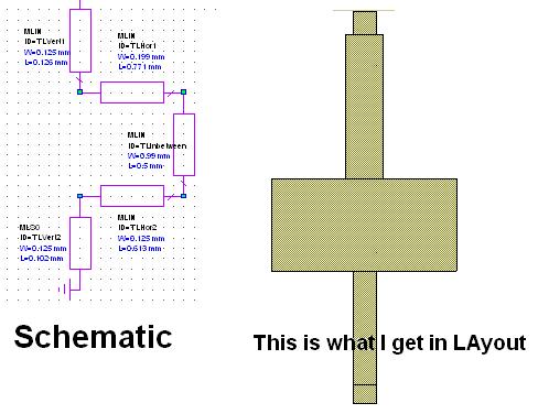
Your schematic consists of 5 lines with no bends, and this is what you get in layout: 5 lines that are connected in series.
The software is designed for microwave applications where the bend has some electrical effect. There are bend/corner elements that you can connect between the straight line segements. These will include the electrical effect of the bend, and also create the desired layout.
---------- Post added at 13:44 ---------- Previous post was at 13:40 ----------
Ok. You can model it the same way. For connection, you can use a "T" junction elements that creates the desired layout.
Yes. The resistor will have some parasitic series L, but that is not a problem for your application.