VNA calibration on board calibration kit
I have to measure the VSWR of an SMD chip antenna. I have built on board calibration kit:
The cable to the VNA is this:
I get strange results from the antenna. I think that calibration kit is correct. Any suggestion? Thanks guy!
One part of antenna is ground in PCB, and from photo I guess that total size of PCB is small.
Your measurement cable will extend that ground-plane quite a lot so total antenna situation will be very different depending if cable is connected or not. How are you compensating for that?
What type of VNA do you use? Assume you can define your own calibration standard in VNA?
The calibration seems basically O.K. The cable will of course affect the impedance measurement, usually it's appropriate to place several ferrite tubes around it. Like shown here https://www.edaboard.com/thread129541.html#post567000
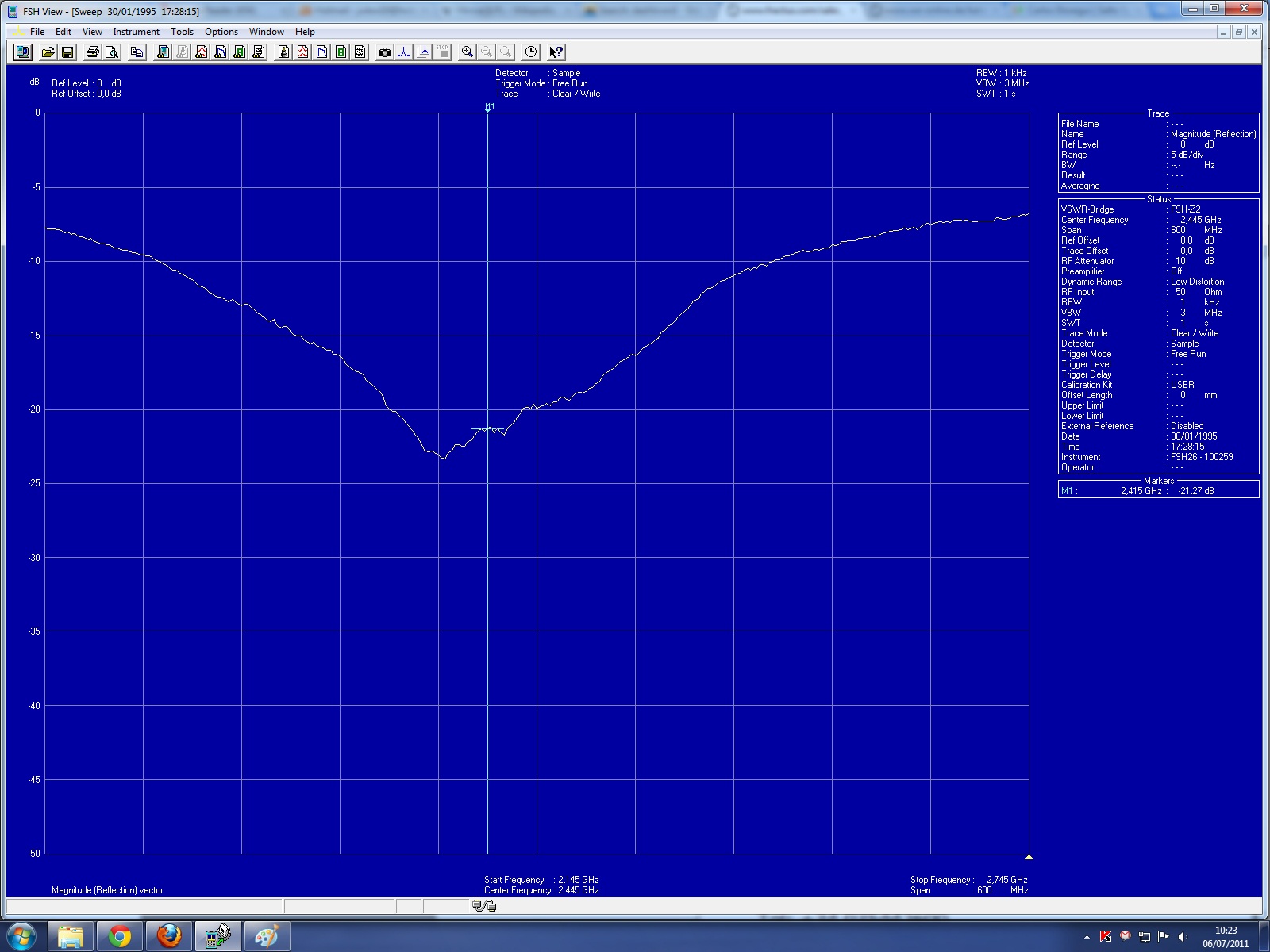
Can you show the S11 measurement? Some ceramic antennas have high Q and are very sensitive to proximity effects. There usability for regular communication applications is rather limited.
Hi,
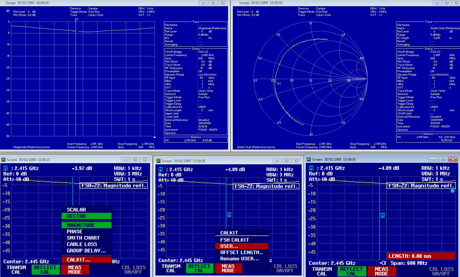
Here is my complete setup:
As you can see i don′t use any ferrite. Maybe it is very importat in my measure. Are ferrites cancelling ground extend effect?
VNA is the Spectrum Analyzer R&S FSH6 with FSH-Z2 accesory. You can use USERCAL option and i have it in 0 mm. After cal i have checked SC, OC and load in smith chart and they are in correct place.
Attachment 58365
Thanks! Very usefull your help
There's apparently a problem with the attachment.
Ferrites can reduce the cable effect but not exactly cancel it. It can be best viewn on the VNA display. If touching the cable and moving the ferrite tubes doesn't change the measurement, the effect can be expected acceptable small.
I see from the VNA display, that it's a 2.4 GHz antenna. For this frequency range, the ground plane has already reasonable dimensions and the cable effect won't be expected very strong.
Hello,
Here the attachment:

Do same measurement but replace antenna with 30 mm wire just to check if it is something wrong with current antenna.
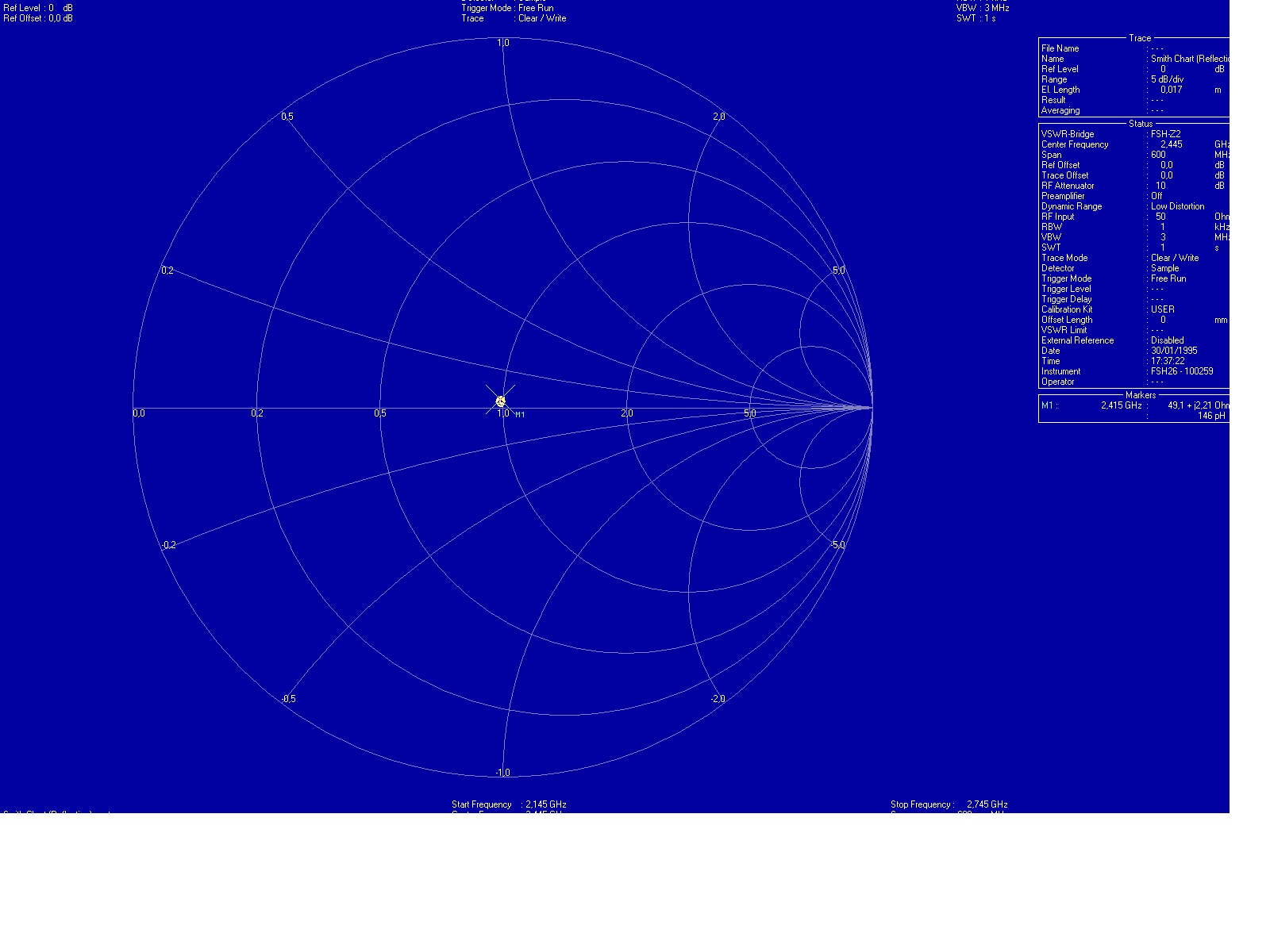
I understand, that the Smith chart is displaying a S11 measurement, so 50 ohm matching should be at the center. Do you see your 50 ohm calibration resistor at this location? Did you check, that it's actually 50 ohm?
This is complete mismatch in any case, either wrong calibration or defective/wrong connected antenna.
Hello,
Here 50 ohm:

I have check te lamda/4 wire antenna and the result is OK!

Maybe there is a problem with antenna position but we have just copied the datasheet.
http://www.fractus.com/sales_documen...S1_N_0_102.pdf
Resistive measure antenna from end to end, check for thin breaks, check if soldering pads seems been well soldered.
Hello,
0 Ohm measured with Fluke voltimeter. It is a production unit and it works, so soldering is ok. This PCB is in production for 5 years.
This is very strange... I have test another chip antenna in the same position (Wurth 7488910245) and VSWR is very similar.
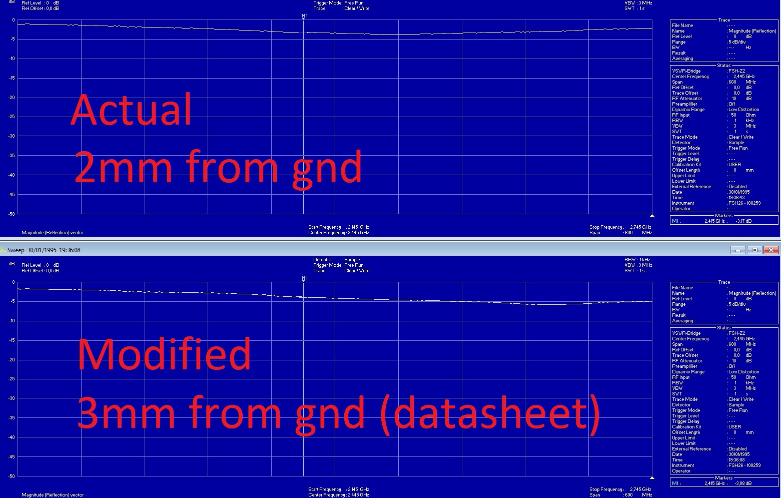
I have been measuring and the antenna is closer to gnd than specified in datasheet. I have move it away from ground and resonance frequency has moved but vswr is very bad.

Hi,
First thanks for your help! A lot of fun this morning...
I have measure the line that goes from microstrip to antenna and it is a little bit shorter than in datasheet (3.60mm instead of 4.75).
You should also detect continuity from the antenna jack to the via on top of the antenna.
I didn't use 2.4 GHz chip antennas yet, my tests have been with Yageo 433 MHz. But even with unsuitable mounting position you would see a higher antenna radiation resistance. The about 10 ohm in the smith diagram looks like a tuned electrical small antenna without correct matching. It may be observed, if the chip antenna is actually broken. Don't know how.
Not directly related to the problem, but why do you have the antenna mounting pad covered with solder resist?
Checked. I have some PCBs and all of them are ok.
I have checked 3 production PCBs and i have resolded one and it doesnt change.
If the antenna's S11 has been correctly measured with 0.2, it would show in a considerable e.r.f. reduction, about 14 dB compared to a matched antenna, which should be apparent.
I can be wrong but the ground area were connector is placed, it looks small. Looks as an isle not connected with other isles on PCB, cant see any vias, looks just as empty holes, is it a dual or single side PCB? In a case as this, I would never use a connector as it can cause so many hidden errors. It is better to sold coax-cable directly on PCB. As impedance is unexpected low in smith diagram, is it a unwanted parallel load somewhere.
Remove some extra trace backward against transmission chip, so it clearly is cut. Using ferrite beads around your cable is a good practice, always. See the PCB picture here.
The gound area is connected with vias. It is dual pcb. It is a copy of a Texas Instruments reference design.
I use connector instead coaxial cable because of the repeatability.
I realise that pcb thickness is not correct. It is 1mm instead of 0.8mm. This can be affect the microstrip transmisión line to the antenna but... with calibration it doesn′t matter if microstrip′s impedance is incorrect. Isn′t it?
I reviewed the information given in the thread and there are some unclear points in my opinion.
- You showed the calibration setup in post #1. I don't see a photo with the antenna reconnected after calibration (with a jumper wire or similar). Did you perform the antenna measurement on the same board after calibration?
- You reported Würth 7488910245 has shown a similar VSWR. In fact, it's intended for vertical mount position without an interconnecting small PCB trace. However, did it also show a similar Smith diagram? Did you test the Würth antenna in a vertical mount position?
- E Kafeman has asked, if the transmitter side has been realiably disconnected in the measurement. I presume it is, but the void can't be clearly seen in the photos.
- I think, the most important difference to the Fractus/TI reference design is the 1.1 mm reduced spacing between antenna and board, although I can't imagine yet an impact as observed in the measurement. Did you try to modify this feature, e.g. my milling or cutting 1 mm copper pour from top and bottom side or placing the antenna at a more distant position, connected by a wire?
Best regards,
Frank
P.S.: I just realized, that the mounting distance is different in the TI and Fractus designs. TI is (if not a typo) very near to your present dimensions. The VSWR numbers are almost comparable (TI somewhat higher), so both seem to work. No S11 measurement is shown for it either.
Yes. The antenna is connected to feed point. Here the PCB i use:
I haven′t test it in vertical.
Yes the transmiter has been disconnected removing inductor microstrip with a Dremel.
There is a distance diference in datasheets: 1 mm. I moved the antenna 1 mm with the same trace lenght and modifing pad. Same results. TI recommended us to use their AN.
We have another PCB with different thickness. The thickness in the current PCB is incorret so microstrip lumped elements and the final microstrip line are wrong matched. I mean, their Z0 are different from the original reference design. We have to correct it but actually it shouldn′t affect my measurements i think because i calibrate VNA after transmision line.
Thanks a lot all you are helping me!
That's clear so far. I wondered, how the antenna had been connected after calibration, and if it's been measured on the same board.
Yes, the difference is in a slightly higher capacitive load to the antenna connecting trace and the antenna itself. It can be expected to de-tune it somewhat, but not to change the impedance drastically. The interesting point is, that antenna seems to be still tuned, but strongly mismatched.
Something is obviously very wrong, but I don't see presently what it is.
