BPF design using ADS 2009
I'm a beginner.I have just started designing filters using ADS 2009. I designed a six element band pass filter. But the response is not smooth. Wat am i supposed to do ? Thanks in advance :)
hi check this
http://www.ashokpm.org/Project_report/BPF_Report.pdf
---------- Post added at 23:10 ---------- Previous post was at 23:08 ----------
The MINT Channelizer Intro
---------- Post added at 23:12 ---------- Previous post was at 23:10 ----------
http://post.queensu.ca/~saavedra/ele...torial%202.pdf
http://ecadigitallibrary.com/pdf/CAR...KIM-KREI_a.pdf
* It would much help if you could show us your circuitry. Otherwise, it seems to be problematic to give any comment.
* Your response is "not smooth"? Time or frequency response? What do you want resp. expect from your filter?
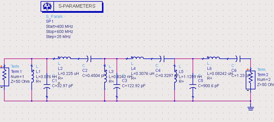
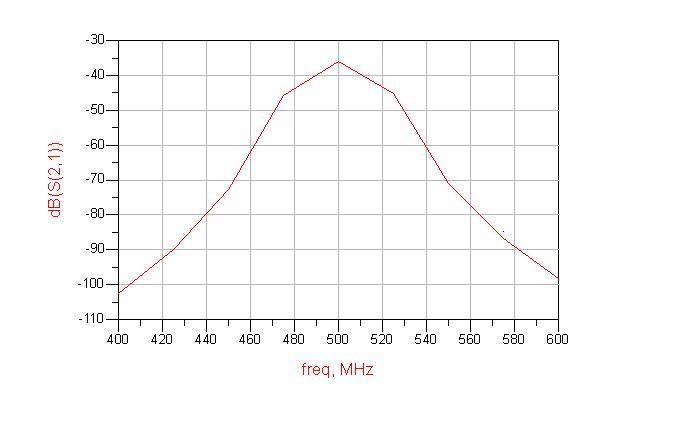
I have attached my circuit and the frequency response. Thanks for your reply :)
You can optimise the your design in ADS, and you can set the S21 range for optimising flatness.
Your filter seems have problem, its S21 < -30dB, that should have problem normally in design. The S21 normally is several dB.
Set a smaller frequency step, so that you can see what happens in the passband. At the moment, you only have 3 data points there.
Yes, you need much more data points for evaluating the frequency response.
In addition, what are your requirements - that means, which filter characteristic (ripple within the passband) do you want?
@All
Your reply was helpfull. Can you tell me how to create the layout using ADS 2009 ? Do we have Auto- layout ?
For ideal lumped components? No.
How do we create layouts if we use lumped components for the design ?
I used to simulate in ADS, and then verify in AWR, then export AWR layout in DXF format. The dxf can be imported into Altium for PCB.
i'm have a few suggestion
if you simulate the BPF ,
Simulation set sweep point up to 201 or 401....
maybe can solve your question .
Have a look at the ADS examples, like examples\RF_Board\cellular_pamp_prj
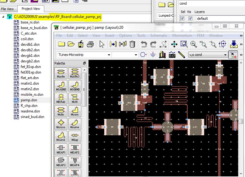
@volker_muehlhaus : Where should i look for this example ? Is it possible to create layout with lumped components design ?
It is part of the ADS examples. You can see the path in my screenshot.