Export geometry from HFSS to Altium
I have a structure in HFSS and I would like to export it on Altium v8 in order to create the associated PCB. Does anybody know if there is a method to do this maybe using some standard output file?
Thank in advance,
Matte
Hi Matte
Try to export from HFSS in Autocad dxf format and import to Altium with
same configuration (mm or mils). You can also try converter like
LinkCAD.
Good luck!
Hi micro,
thanks for your reply.
Actually this is what I tried to do. Export as .dxf from HFSS and than try to import it on Altium from the File-Import-DXF_File. But I get the following error: "CAMDXP: invalid .dxf file".
What is strange is that sometimes it works.
If I open the geometry file with Cad it seems to be correct. I post you the file:
ex.zip
Thank you
Best,
matte
Do you know about the DOS-UNIX style end-of-line issue (CR vs. CR-LF)?
Your DXF file is UNIX style end-of-line, which might cause trouble on a Windows system, depending on the program. If you open it in the Windows editor (notepad), you will see that it's all in one big line, with no line breaks.
If this DOS<>UNIX file format is the problem, it can be solved with UNIX-to-DOS conversion tool that fixes the end-of-line character.
I have done that conversion. Try the attached file.
Hi volker,
thanks for the advice, but I get still the same error...
Ok, but I can confirm that the file is valid DXF. It does read properly with my DXF readers.
Around your rectangular spiral, you have an additional frame.
I wonder if that causes problems in the Altium reader because it overlaps with the spiral on the same layer.

I tried taking away the external frame but nothing changes. But what is really strange is that for the same .dxf file, it worked the fistr time I imported it and no more ...

I think it's a bug from the version I use of Altium...anyway I converted the dxf file into a HPGL file and it works!
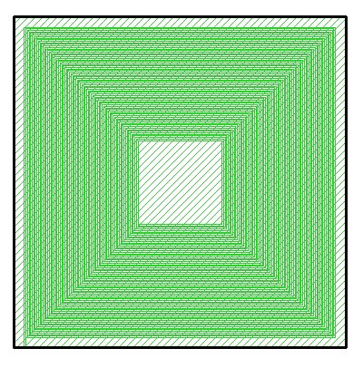
What I get is:

Now I have to fill all the geometry and transform it into a PCB...any suggestion?
Hi Matte
I think that import module dxf is one of the worst parts of Altium. In
attachment I sent you converted folders to Gerber format
Hi Micro!
Thank you very much, your files work perfectly and the conductor trace is filled now!
Can you tell me how to convert the .dxf file into this Gerber file?
Thanks,
Matte
Hi Micro,
checking the imported geometry I realized that the trace width and spacing are different from the original (both in CAM and PCB documents)..The original geometry in HFSS and Autocad hadwidth = spacing = 0.15mm and now they measure width = 0.2 and spacing = 0.1.
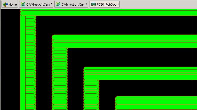
In addition the inductor's trace looks very strange, composed by several smaller conductors as you can see in the picture:

What happend to the original sizes?
What you see are typical effects in DXF to Gerber translation, where areas are filled with many small strokes.
For your simple layout, the easiest solution is that you just use the outline from DXF import, and redraw the inductor manually with a 0.15mm trace. This should not take more than a few minutes.
So, no way to semplify this "conversion"? The only way is to do it manually..? Maybe filling the traces before the conversion?
Trust me, I have worked (programmed) quite a bit on these layout conversion tools for RF/microwave. One of my customers was Ansoft ...
In your case, my advice is to redraw the coil manually with a simple trace in Altium. Because your layout is so very simple and not critical, this is the most efficient method and will only take a few minutes.
If this was a dimension critical microwave layout and the exact shape of the bends would matter, it would make sense to think about an automated way. In your case, manual redraw is the easiest solution.
Hi Matte,
I'm replying late because I didn't have time.
volker_muehlhaus is an expert in this topic and is right in what he's saying.
You can easily redraw your simple layout manually. It's harder if you redraw more coplicated layouts. I tried to do as fast as possible conversion of your file and that's why I didn't check the scale of it. In attachement you got correct file.
I'll explain you step by step how I do it. I'm working with making PCB technology documentations. So that's why Gerber files are the easiest for me to work with.
Firstly, in microwave software I draw simple layout, for example like yours. Secondly I import it to software to manipulation Gerber files (like CAM350 or other). Then I check sizes of the imported layout (I forgot to do it while making your file). If the sizes are correct, I work with these files. If they are not, then moslty option of import DXF files has possibility to scale. I use it (warning! scale may be in incomplete number, for example 0,8453) and I check the size again. If it's correct, then it's finish checking. If it isn't correct or not standart (different for x and different for y), I import DXF file as it is. I'll have posibility to correct dimensions at the end of my work, because in software to manipulation Gerber files, very often there's option to scale Gerber file for x and for y this means that at the end of my work I'll have correct size.
In the next step I use one of the Gerber software options which is "filled polygons". Different softwares has it own different filled polygons and mostly this information is lost while importing. If the information isn't lost just delete it, because it may use apertures which photoplotter may cannot draw. So I use filling by Gerber software because I'm sure that photoplotter will correct light film for making PCB. For high precision I use 2 mils width line for filling. It's a vector filling, which is possible to use even by very old photoplotters.
It's complicated work and you must do it individually every time. volker_muehlhaus is right that in simple works its easier to do it manually.
I hope that my English was clear enough and that it will help you in your work.
Good Luck!
Hi Micro thank you for your precious advice but the geometry dimensions still don't agree with the original design, they are 200mm and 100 mm..actually my interest in the possibility of autocreate a PCB from HFSS was due to the fact that I have a lot of geometries to produce, so even if they are very simple I would be greater .
At this point I will design in manually..
thank you everybody
Guys
this is a very interesting thread.
The general problem is to export the geometry found in a microwave CAD (HFSS or ADS or others) to a PCB tool.
I've always found a lot of problems using DXF, similar to the one you mention here.
In my career I've found the same issue many times, and the manual solution has been the most practical one.
Today I know that there is an integration between Agilent and Cadence (Allegro), but it is given as the highest price options (several kS), not really affordable if you don't you it daily.
I would like to ask you (especially to volker_muehlhaus) if you have suggestions, what is the most used solution for this issue based on you knowledge.
Mazz
The problem is that your DXF objects (LINE, POLYLINE) describes the exact outline of a filled area, but many PCB tools have no equivalent for that.
One approach is to fill the area with many small strokes, as seen in post #11. This is compatible with traditional Gerber fiel format, using many small lines.
Another approach is to use the Extended Gerber RS274X commands G36/G37 , which describe polygons. This way, you can define the filled area by the outline, as seen here:
What's All This About RS274X Anyway?
However, your PCB tool will use a certain line width to draw that polygon boundary. If the PCB tools just follows the outline with that "wide line" and does not apply an offset, your filled area grows by 1/2 line width. The only "trick" you can use is to define a really thin line for that polygon, to minimize the error.
