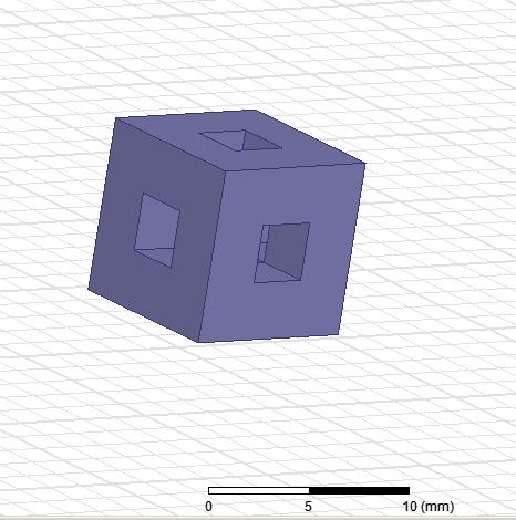
Power absorbed by fractals
Now i have a problem in an EM model to define the EM power absorbed by a fractal structure. Simulators chosen are HFSS and CST MWS. In both simulation tools, i define a model by sending incident plane wave torward the structure. I define 2 wave ports (each port is far from structure face by 2*lambda) and the boundary is PML (far from structure face by lambda/4).
The problem is that there is transmission direct from port 1 to port 2. It means that i can never find the absorbed power with an acceptable precision.
Please anyone got any idea, please share your opinion
I don't think you should define ports far from the structure.
One port touch the front face of the structure, and the other port touch the back face.
Thanks very much for your idea. I also tried this method. However, it raised another problem of scattering. The EM wave scattered in the structure can escape via other 4 faces (beside front and back face). This mean that we still cannot find a accurate EM fields concentrating inside the cube.
Another method is each port for each face. So there're 6 ports to be defined. What do you think?
I recommed you building your models according to your situations. If you want to test the EMC effect, such as in EMI absorbing room, you should build more fractals models, not just one, to simulation. Such as you build a box, all arrounding with the fractals. Then you can calculate with just two ports.