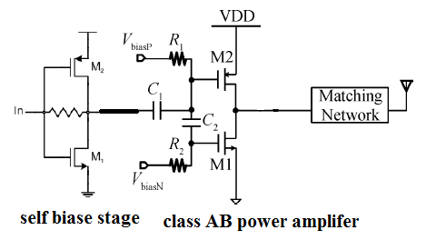
Power amplifier (self biased inverter)
i am working on MICS band application , and I have to design a Power amplifier that can deliver 500 uwatt power to antenna(50 ohm).
i have gone through some IEEE paper and i found that most of them were using Class AB power amplifier which is driven by a self biased inverter. and it is also mention that they are using that self biased inverter to reduce second harmonics and they are using that as a buffer.
i have attached the circuit diagram below.
please help me in finding out
1. How that self biased stage is working (that means is it a buffer stage or an pre-amplifier stage).
2.How it reduces the second harmonics.
If anyone provide me some study material then i am really thank full.
2. A push-pull amplifier will cancel even harmonics but not odd.
Frank
2nd harmonic (that was mentioned in the initial post) it is an even harmonic.
The bias stage is not shown in the schematic...only the driver and the final stage (capacitive coupled)
Vgs1+Vgs2=Vdd and Vds1+Vds2=Vdd so...
Vgs1+Vgs2=Vds1+Vds2=Vdd
Transistors are in saturation mode so that autobiasing conditions are met...
hiiiii vfone...
there is no bias network for that for Power Amplifier part,it is a Class AB stage so it is biased by bandgap reference circuit by generating 1.3 V Pmos ,and 0.5 Nmos.
and first stage is self bias stage because of feedback from output drain terminal to input gate terminal via a Resistor.
my doubt is: In order to make that self bias inverter we need to connect Capacitor between gate terminal RF signal input. and how it reduces the even harmonics.