How can I design a Return to Zero optical link
I want design a Return to Zero optical link with variable duty cycle.
I started it from 50% duty cycle.
Following is my block diagram. Basically, I use a and gate to generate 50% duty cycle Return to Zero(RZ) signal
and use D flip flop to recover the signal to Non-Return-Zero.
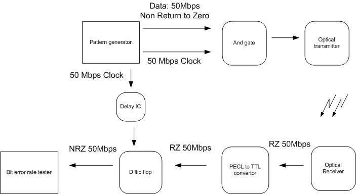
So my question is , are there some off-the-shelf RZ/NRZ converter ? (I prefer not to use this D flip flop)
I can find the NRZ/RZ converter, for example, HMC706LC3C or 13706RZ-S02L.
I can also find a discontinued RZ/NRZ converter, like SHF 315 P...
or any options on this optical link ,
or some design guide for Return to Zero optical link ?
thanks all .
To detect this protocol requires a mixer with clock recovery signal. Digital mixer uses D FF but is sensitive to noise and does not use all the energy of the bit.
other method uses analog multiplier (non linear amplifier with clock * Data.) clock must be in phase (PLL)
Good luck. why use RZ code? why not use something else?
50Gbps FF here http://www.inphi.com/images/pdfs/Inp...2011-11-08.pdf
It wasn't advertising, rather direct contact info with the company that is developing this new detector and many jobs open to develop these new parts.
Perhaps beyond scope of your project to develop this solution. But you can purchase one below.
SHF has other designs that are complete products with clock data recovery.
http://www.shf.de/en/communication/p..._and_receiver/
They use ASK and DSPK.
Hi, SunnySkyguy, can you explain this in detail, or introduce some Literature to me.
why detect this protocol requires a mixer with clock recovery signal?
---------- Post added at 12:19 ---------- Previous post was at 12:18 ----------
I looked at this devise, they are works at high frequency up 10G, but my link is only 50-200M, besides, it is too expensive...
TO integrate all the energy in the data bit modulation and recovery clock with low jitter and best BER you need to use a mixer and matched filter.
Otherwise if SNR is very high, you can make something work with delay and 200MHz FF
I'm under the impression that you are missing the simplicity of the intended operation behind the terms and various IC specifications. Sketching the involved waveforms may help.
When are proceeding to a real wireless link, clock recovery has to replace "Delay IC" clock path in your diagram.
This is an optical high speed communication link not a logic circuit.
As such primitive time delay re-sync circuit is not recommended unless just for lab use.
High speed Optical link with rubust Bit Error rate should consider stable clock recovery,
My initial post was accurate. YOu might prefer a quality transimpedance amplifier, PLL clock and data separator circuit for reliable data.
I believe this is also called ASK protocol, am I right? or RZ-Mark
Sorry for possible misunderstanding, I was referring to the initial post and the respective diagram, not your suggestions. I completely agree, that the setup for a real optical link, without knowing the clock a-priori is not simple.
OK if I understand correctly , you basically suggest 2 things:
1, use a CDR(clock and data recovery) instead of the "delay IC+ D Flip flop",
my question is why I need this recovered clock ? I can directly get clock from my pattern generator...
and even I can get this low jitter 50Mbps Clock from CDR, I still need a delay IC and D FF to change the 50M RZ Data to 50M NRZ data.
or do you mean, if the input of CDR is 50M RZ data, the output will be automatically change to 50M NRZ data and 50M clock?
2 use a mixer to integrate all the energy
what kind of mixer do you mean ? a frequency mixer ? I am sorry I never heard this, can you introduce me some book of documents about this.
Simple answers:
1) Clock noise adds to data recovery error, so make it stable as possible.
2) mixer in frequency domain is a multiplier with matched filter bandwidths,
also, mixer in time domain it is a phase detector, in analog domain, it can be implemented, in digital domain it assumes optimal analog signal processed already ready to decimate into digital binary data.
now for a lecture... which may be redundant
There are dozens of baseband communication methods in both Analog and Digital domains.
Amplitude, Phase, Frequency methods in general leads to many more, each with tradeoffs for simplicity and performance.
In the digital realm, the signal is assumed to be noise free so SNR is not an issue, but in optical communication as in any long distance method, as in wireless or wired too, the signal is analog at some point and thus gathers noise and loss of signal contributes to SNR figure. SNR is directly related to BER on a logarithm scale. So on can value can often be calculated and correlated to the other and proved by Shannon's theorem.
So if you are only concerned with digital modulation ( ideal SNR ) ignore my comments, but real channels try to optimize SNR of received signal.
THis also includes SNR or jitter of the clock recovered from the data as excess phase error between Clock and Data can result in a decoding error.
Once this is understood, communication theory proves, helps how to improve reliable communication as fastest rate, unlike this reply. ;)
Then optimize the channel filter to the bandwidth of the data and clock.
Some modulation methods contain DC and others invert phase after a number of bits called run length limit or RLL to avoid DC in the signal.
High speed data systems use this such. Increasing energy in the clock transitions improves SNR on recovery the clock at the expense of maximum bit rate ( low error in phase and freq., fast capture speed of PLL etc) This is why RZ is often used only in optical, since bandwidth is not the limiting factor, it may be jitter from optical path.
Some modulation methods improve SNR at the expense of upper bitrate, complexity, cost, power level or other factors.
There are volume of books on each subject mentioned above.
So one has to defined the requirement for SNR and the channel communication before choosing a receiver method.
To optimize on Optical distance before repeaters are required, this is very important.
In a lab just for ease of understanding one way to do it, it is less important.
THis is what I remember. THe details , you may choose research or not.
You can find volumes of information on the web for communication by any combinations of the following keywords:
matched filters, modulation (analog, digital), Shannon's Theorem, Baseband coding / conversion, CDR, PLL Clock recovery, eye pattern, BER, Nyquist ISI
etc.etc
I am sure you can learn to find them. This is the purpose of your education is to learn "how to teach yourself".
But let me say I recall a solution I once used that uses a PLL to phase lock a stable clock to the center of data eye pattern others than lock to the center of the data edges or data transition window. Once you have a stable clock ( useful for both async and synchronous channels) you can filter the data to reduce jitter, phase shift, group delay distortion and thus chance of error from jitter ( or marginal SNR) YOu can correlate in time or frequency domain these values.
Now for an example of my quick web search...
basic reference... http://www.perihel.at/2/basics/01-DCOM_Basics.pdf ...
definition>> http://en.wikipedia.org/wiki/Nyquist_ISI_criterion
=Simulation results in general http://www.docstoc.com/docs/48405534...-rossir24-0019
> One implementation method > http://www.docstoc.com/docs/27439340...con-Integrated
that concludes my sermon. now seize the channel
Thanks very much for your patient replay, after reading one of the basic documents you suggest, I find it extremely helpful. I will read them all, and then looks back to my problem.
Anyway, thanks very much.