enabling bias to my LNA
Please help?
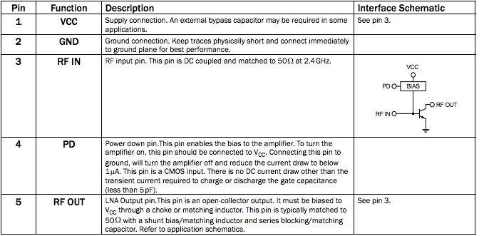
Bias circuit is nedded to stabilize the OP of the transistor against temperature and/or process variations during manufacturing.
Because LNA has probably been optimized just for this OP and this must be maintened all over operating conditions.
Bias element might be simply voltage/current regulator or more complex temperature compensating, process insensitive etc.circuits.
SInce my RF input pin will be connected to the port 1 of my vna is that incoming signal AC in nature?
If it is AC signal signal in nature I want to place a series cap between the input pin of the LNA and the VNA to prevent any DC offset?
If I did not include a series cap between the VNA and input pin of the LNA what is the ramification of the DC offset?
Look at the application note of that IC.There may be a coupling capacitor or not, I don't know.
If there isn't, you should connect a series cap to block the DC level from VNA ouput.This is valid for output too.
Cap values are/might be subjected to frequency of interest and input/output impedances.
Read application note and apply the circuit on your board.