Need help understanding an LNA design method
If you look at page 20 at the end of the first paragraph they say, "The battery is connected to the 5 Ω resistor
and 0.1 μF capacitor junction in the final circuit." If they connect the capacitor in series with the battery, then they are going to block the DC power to the drain, unless the capacitor is in parallel with the 5 ohm and 27nH inductor, right?
Another question, if you look at page 49, why do they use the ideal feed inductor and 5 ohm resistor that connect to the drain? Why couldn't they just have connected the 27nH (RF choke) coilcraft inductor where the ideal inductor is? Instead they place the same series circuit that suppose to go to the drain and place it off to the side near node 3a. I understand that they are trying to represent the actual component response, but when they place the circuit near the battery, then the 0.1uF capacitor will block the DC component, which kind of leads to my first question. I hope you can understand my question, thanks.
What they mean is "the battery is connected to the junction of R5 and C2"; i.e. the 0.1 uF cap is parallel to the battery.
I think R5=5 Ohm represents the Internal resistance of the Battery for that they aim, but C2=0.1uF is not very meaningful for s-parameter simulations at higher frequencies.
This may be used for a real (!) model of a Battery but I have never seen such representation including "series capacitor" ?
If the component was an Inductor, OK, it's pretty comprehensive but it seems to me a bit weird.
Second question has a simple answer.
The model of Coilcaft may create Convergence errors while the circuit is simulated under non-linear conditions.
Big Boss I have two questions, one: where did your name come from? And two: about Skatefast's post on his link. I was reading on page 20, it mentions..."Note in Figure 17 that the “cold” end of the 27 nH inductor is connected in series with this 5 Ω resistor." Do you happen to know what they mean by the "cold" end of the inductor and if it has to do with the current travelling from hot to cold or vice versa? Thanks.
Hi biastee, you mean something like this?

I guess the 0.1 uF capacitor would be a bypass for lower frequencies, since its next to the battery, right?
@skatefast08
Correct. The functions of these components are explained in the ATF-54143 appnote: AN1222 pg. 3, (https://jp.broadcom.com/docs/5989-2273EN)
Although one poster speculated "R5=5 Ohm represents the Internal resistance of the Battery", the resistor is actually used to stabilize the ePhemt at very low frequency, where the reactance of the 27 nH inductor become insignificant. See AN-A001 (http://www.hp.woodshot.com/hprfhelp/...her/ana001.pdf). The "HP" on this appnote is because it is the original name of the ATF-54143 manufacturer.
if you look at page 10 in the article I posted: http://literature.cdn.keysight.com/l...990-3356EN.pdf, the 5 ohm resistor is to bias the transistor at Vds =3V and Id = 60 mA. I believe they are adding that exact resistor, as it shows in the article in addition to the choke, "The ATF54143 nonlinear model has the 3.3 V supply voltage connected to the drain through a 5 Ω resistor Rd. This resistor drops the supply voltage
from 3.3 V to 3.0 V when 60 mA of bias current flows through the drain terminal."
The circuit in post #5 is almost similar to the original simulation circuit from Keysight paper, but not exactly. They apparently wanted to include the parasitic impedance of the 0.1 uF bypass capacitor, thus it shouldn't be shorted by an ideal voltage source. If the difference actually matters should be checked.
Due to the fact that the 27 nH has parallel capacitance, the 0.1 uF capacitor has an effect at high frequencies as well.
I concur with you that the resistor is a physical component that is added to the circuit. You can find that resistor, although of different values, in all the appnotes associated with ATF-54143 - AN1222, AN1352 (ATF-58 is a relabeled ATF-54) and AN1299. (shameless plug) I am somewhat familiar with the last two, having written them.
In the Keysight simulation, the 5 ohm resistor and 0.1 uF cap are modeled as ideal components; i.e. no parasitic. Moreover, there is no attempt to model the surrounding PCB traces. As these components' contribution at high frequencies are already being neglected in the original simulation, it does not matter anymore if the cap is shorted by an ideal voltage source.
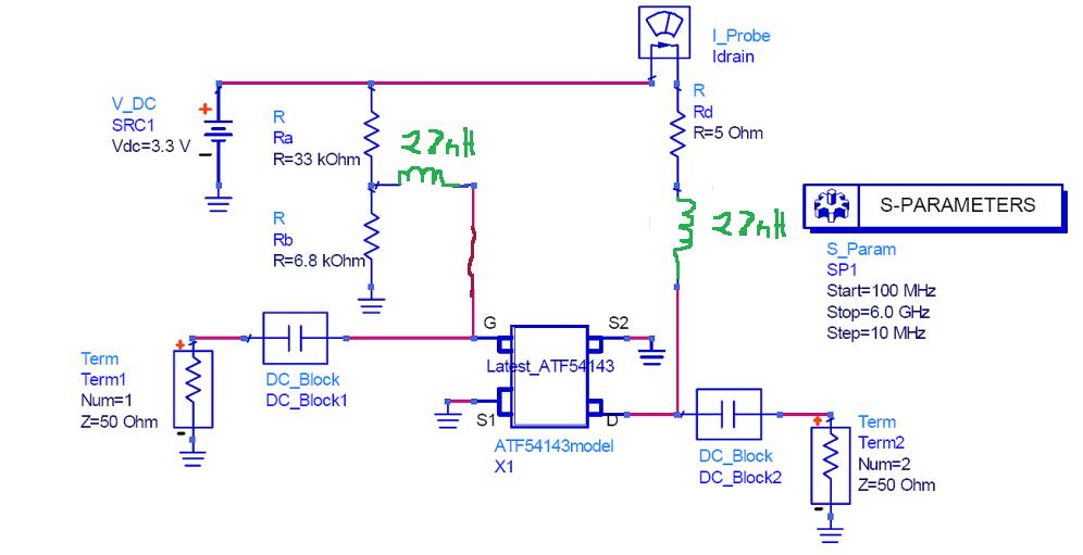
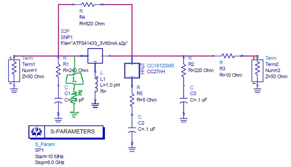
If I want to use another RF choke at the input as shown in figure 1, then would my S2P circuit look as shown in figure 2 instead? I feel that the circuit should look as shown in figure 1 instead of what is shown in the keysight paper as shown in figure 3 or as shown on page 11 (http://literature.cdn.keysight.com/l...990-3356EN.pdf). You can see that I replaced the ideal RF chokes with the 27 nH inductors at the input and output to represent what I would believe would go there in the final circuit. You can also see that I placed a resistor below the 27 nH inductor at the input in figure 2 (painted in green), which I think would represent as the equivalent resistor value of the voltage divider network, just as if it was the 5 ohm resistor that represents the 5 ohm at the drain (which is also shown in figure 3 or on page 11).
figure 1

figure 2

figure 3

I recommend omitting the RF choke from the simulation because it is intended to be "invisible" at 2 GHz. However, instead of obediently following my recommendation, your interest will be better served by comparing simulations with and without the aforementioned choke. My prediction is that the choke will not significantly change the simulated performances because 1. the amplifier with feedback has a low input impedance, and 2. the choke is modeled as an ideal component (no parasitic).
I agree about not modelling PCB traces appropriately. However figure 45 has a capacitor with s-parameter description. I presumed it serves a purpose, not sure if it's a realistic model.
