A Biasing problem in LNA circuit
I have 2 questions reagarding biasing a LNA, as shown in the capture below:
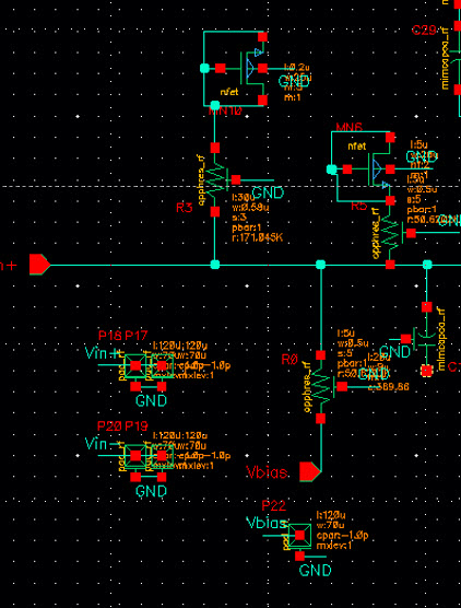
1/ For what i ve known so far, the R0 resistor is employed as a large enough value to restrict the noise current contribution from current mirror into core LNA devices. However, if I have a stable power supply that can be tuned
for biasing G gate. Can I remove the presence of R0 in my design and connect immediately PAD Vibias to the available supply?
2/ I dont know the functionalities of R3, R5 as well as the MOSFET capacitors connected in series with these ones. Do you know what it purposes to ?
Highly appreciate discussions from all /
Thanks,
Aren't all the terminals of the MOSFET shorted togetehr?
1) There is a trade-off at that point. If you increase Rbias you will reduce you stability, increase your gain and decrease your NF.
2) Mosfets are capacitors there (MOSCAPS). I am not why they are used there (maybe for including package parasitic).
But definitely not part of the design !
Yeah, all terminals are shorted together for Mosfet capacitors, that is weird to what i have seen so far. Can i remove the R0 here ?
For 1) because I connect the power supply directly to this PAD to bias for LNA, so can i remove this resistor ? because in term of noise, NF will be improved.
2) To modeling the parasitic of PAD, it is already included in PDK by a specific component of around 50 fF
R3 and R5 for tune gain and NF.
NO. you cannot connect bias directly to gate of transistor. It will short AC. Are you aware of that ?
you need a resistor to separate DC and AC. and decoupling capacitor series with source and input to separate DC.