Designing VGA for 430 to 438 MHz
时间:04-06
整理:3721RD
点击:
Hello.
I'm going to design VGA for :
1.frequency 430MHz to 438Mhz
2.output level signal not going to -40dBm or maybe 30dBm
3. the modulation is FM ,
I searching the reference on searching web, and I find the reference from:
1.http://www.eecg.toronto.edu/~kphang/...martin_AGC.pdf
2. http://www.analog.com/static/importe...ps_Revised.pdf
3.http://www.analog.com/static/importe..._AGC_Loops.pdf
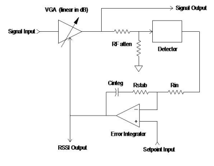
From this references, they use IC ad8361 and external detector ad8361 and From references one until three the block diagram for designning is similiar like this:
I red the references and the datasheet from the ic"s. But i still dont know, how to design it? because:
1. Is the IC ad8367 have satisfying the criteria of spesification?
2. What is the output from detector true rms ad8361? is it dc or ac with spesific frequency, because in the datasheet i dont find it?
3. How about the looping bandwidth for my design?
4. I have read the 2 and 3 reference example.
What is the function of Cin and C which is paralel with Rstab (62K in this picture)
5. How to calculate the set point?
6. I dont know, about the zener? from this picture is 12 V but the input is 5 V, why is 12V zener used?
7. And the last? How to measure the AGC?
I hope we can discuss it in this forum, or you can send it to my email. gambling.3@gmail.com
Thank you for your attention.
I'm going to design VGA for :
1.frequency 430MHz to 438Mhz
2.output level signal not going to -40dBm or maybe 30dBm
3. the modulation is FM ,
I searching the reference on searching web, and I find the reference from:
1.http://www.eecg.toronto.edu/~kphang/...martin_AGC.pdf
2. http://www.analog.com/static/importe...ps_Revised.pdf
3.http://www.analog.com/static/importe..._AGC_Loops.pdf
From this references, they use IC ad8361 and external detector ad8361 and From references one until three the block diagram for designning is similiar like this:
I red the references and the datasheet from the ic"s. But i still dont know, how to design it? because:
1. Is the IC ad8367 have satisfying the criteria of spesification?
2. What is the output from detector true rms ad8361? is it dc or ac with spesific frequency, because in the datasheet i dont find it?
3. How about the looping bandwidth for my design?
4. I have read the 2 and 3 reference example.
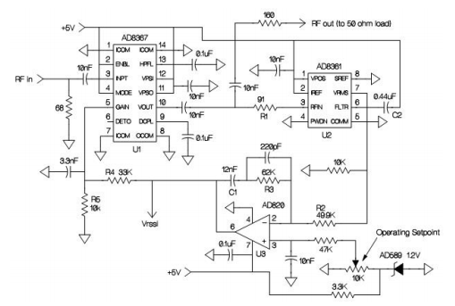
What is the function of Cin and C which is paralel with Rstab (62K in this picture)
5. How to calculate the set point?
6. I dont know, about the zener? from this picture is 12 V but the input is 5 V, why is 12V zener used?
7. And the last? How to measure the AGC?
I hope we can discuss it in this forum, or you can send it to my email. gambling.3@gmail.com
Thank you for your attention.
- [moved] HELP Testbench VGA CORE for AGC 10gbps
- Vector Modulator vs VGA+Phase shifter
- Help!low noise VGA with 40MHz~90MHz bandwidth, 32dB gain range with 0.5dB gain step
- Designing split ring resonator
- Which transistor need to be chosen for designing KU-Band LNA Design high gain, low NF
- Designing an LC delay line