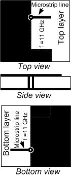
connecting top and bottom layer microstrip lines with a plated through hole A11 GHz
时间:04-06
整理:3721RD
点击:
Hi,
I got a 11 GHz signal in a receiver design and I'm planning to use both side of the RF PCB due to space constraints.
The 11 GHz signal is coming from antenna through a 50 ohm microstrip line on the top layer.
Is it possible to have a plated through hole to get this 11 GHz signal to the other side (bottom layer) of the RF board?
To carry this 11 GHz signal, then is it possible to have another microstrip line at the bottom layer?
If this is possible, on what should I pay attention when designing this plated through hole?
can I have a hole at any size or should I use standard drill sizes and standard copper thickness inside the plated hole (17 um or 35 um)?
Please see the attached image to understand my problem..
cheers,
per_lube
it is possible to have rf signal layer on both sides (top and bottom) but for this to work properly and be manufacturable you would need a 4 layer board stackup. Top and bottom would be rf signal layers and inner layers would be ground layers. It is not very practical but it is possible.
As for the via itself you need to keep it as short as possible to avoid parasitic inductance so the thickness of the whole board needs to be minimal. Via pad size, via diameter and anti pad size will determine the impedance, which obviously needs to be 50Ohms.
layer microstrip connecting 相关文章: