DC supply layer under the main circuit
So i'm new at designing RF circuit and i'm supposed to design a transciever on an RO4003C substrat with microstrip technology and we want to add another layer of FR4 where all our DC supply will be.
So until now I did my designs only on the RO4003C thinking another layer of FR4 under the ground plane wont bother my circuit. but oh boy was i wrong! i have simulated the filter with my substrate and a layer of FR4 below and my losses went from 1.2 to 1.7. and i was wondering why did it changre the results since there is a ground plane between the two layers? and i would also like to know if there's any technics to remedy to these changes.
Thank you in advance.
just to clarify...you had a bottom layer that was DC circuit, a middle layer that was pretty much solid ground plane with only a few "thru vias" and NO big cuts across it, and the top layer was RF?
It should have worked. Could be that your top dielectric layer was too thin...and your dielectric comprised mostly pre-preg glue? Or the board shop did some odd stuff...like instead of starting with a normal RO4003C board with metal on both sides...they instead started with a FR4 board and "glued" an RO4003C board on top with only one metal layer?
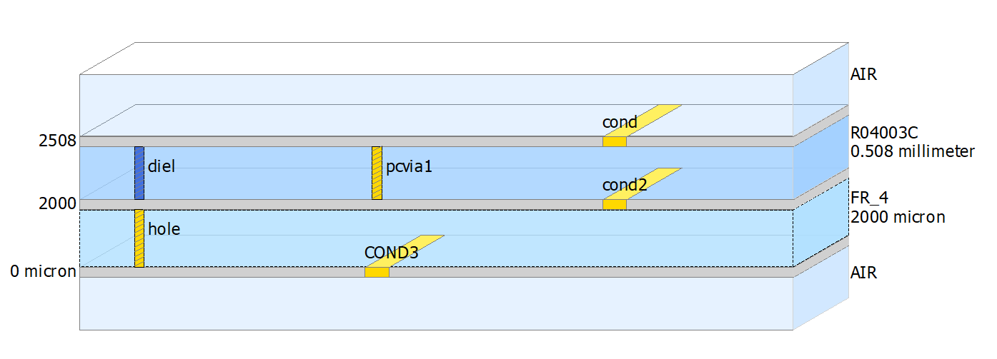
This is how i defined the substrate, you also have the height of each dielectric. do you think it's too thin? and how does the thickness of the substrate play a role in the changes?
We still didn't fabricate the circuit. the changes i noticed were from the EM simulation on ADS.

that's a 20 mil thick board....should be thick enough as long as it is mostly BOARD, and not PRE PREG glue comprising that 20 mils of thickness.
did you make any cuts in the ground plane layer?
If the pour on your inner layer was solid, then that should effectively screen your RF fields from reaching the FR4 substrate. Can you show your PCB artwork for the three layers?
No, the ground plane is a rectangle that covers the whole layer.
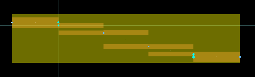
I tried it on a simple coupled edge filter since it's sensitive to parasitics, and here is the layout:
That doesn't clearly show what's happening on layers 2 and 3. Are they both solid planes? Which one are you defining as GND in your simulation?
The Lines are defined on the cond layer, The ground plane on the cond2. on the cond3 there's nothing as i just wanted to see the influence of the FR4 on the filter. I hope i'm being clear.
Possibly wrong EM simulation. In real life, the ground should do the shiedling job.
I noticed that you used flat sheet (zero thickness) metal in your Momentum substrate. In this case, the ground layer is represented by only one current sheet and currents from one side will be "visible" on the other side. This is different from reality.
Also, metal below the ground will influence the meshing of the filter. That might change your filter response if meshing of the filter itself was too coarse.
Ok, I just read this now ... then it might be as simple as a different setting for material properties between the two Momentum models.